Potted electronic component and method for its manufacture

Inactive Publication Date: 2011-05-19
DELPHI TECH INC
View PDF4 Cites 6 Cited by
  • Summary
  • Abstract
  • Description
  • Claims
  • Application Information

AI Technical Summary

Benefits of technology

[0013]The invention enables an electronic component to be potted in a housing with a space left between

Problems solved by technology

For example, the housing may contain electronic or other components in addition to the component desired to be potted that will be adversely affected by contact with the potting material.
Alternatively, parts of the component being potted may be adversely affected by contact with the potting material, e.g., where the component being potted is an electronic circuit board is a printed circuit board having components mounted thereto that may be disturbed by shrinkage of the potting material during hardening or differences between the coefficient of thermal expansion between the potting material and the circuit board when exposed to heat during operation.
Such a space or gap may provide the necessary isolation for certain components in the housing, but can result in bubbles being formed in the

Method used


Image

  • Potted electronic component and method for its manufacture
  • Potted electronic component and method for its manufacture
  • Potted electronic component and method for its manufacture

Examples


Embodiment Construction

[0021]Referring now to the Figures, where the invention will be described with reference to specific embodiments, without limiting same.

[0022]The method and electronic component assembly of the present invention is disclosed in an exemplary, non-limiting context of a printed circuit board disposed in an housing such as a cavity in the solenoid body of a pressure switch assembly in an automotive transmission, although the invention can be applied to virtually any potted electronic component in any housing.

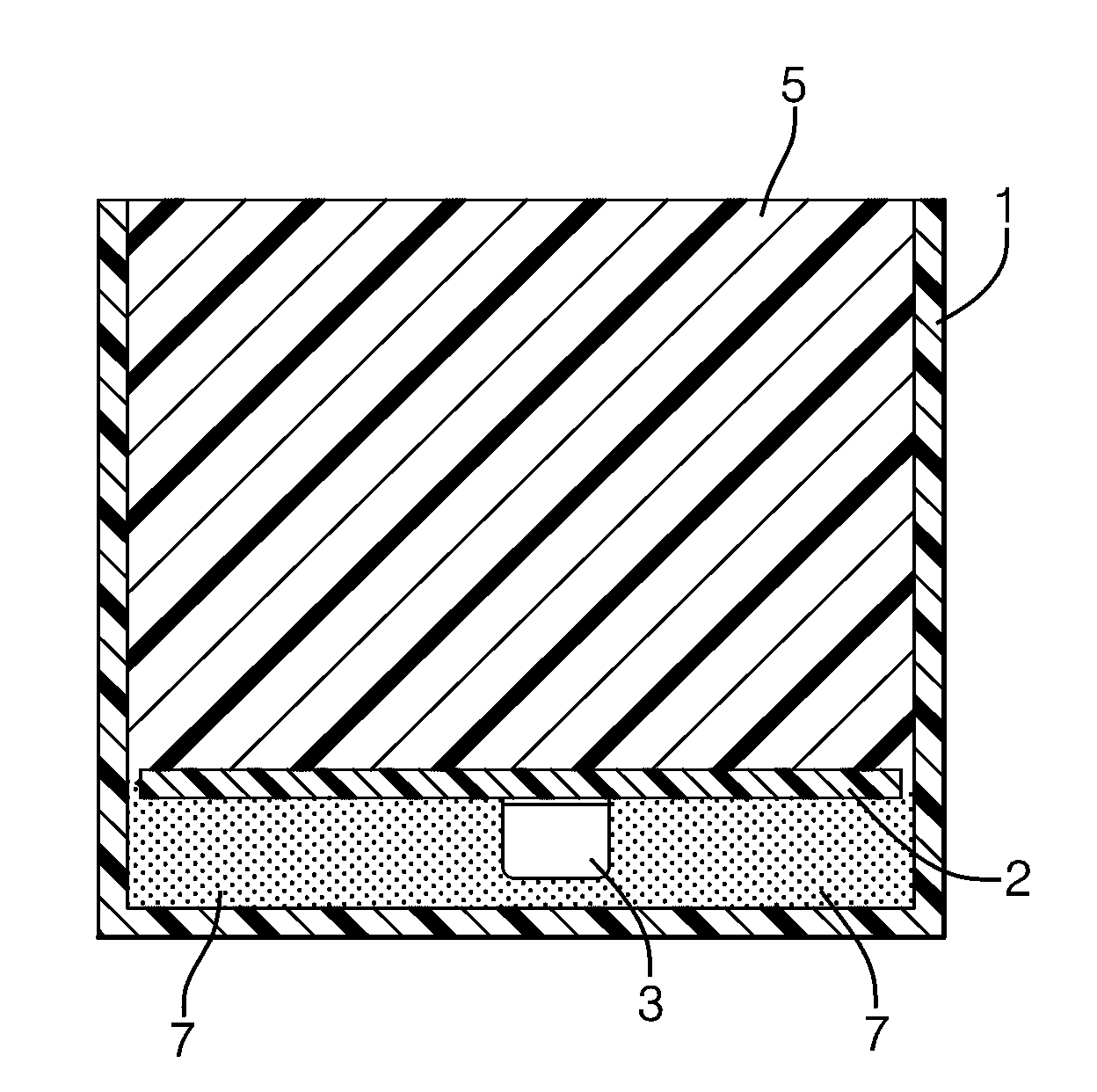
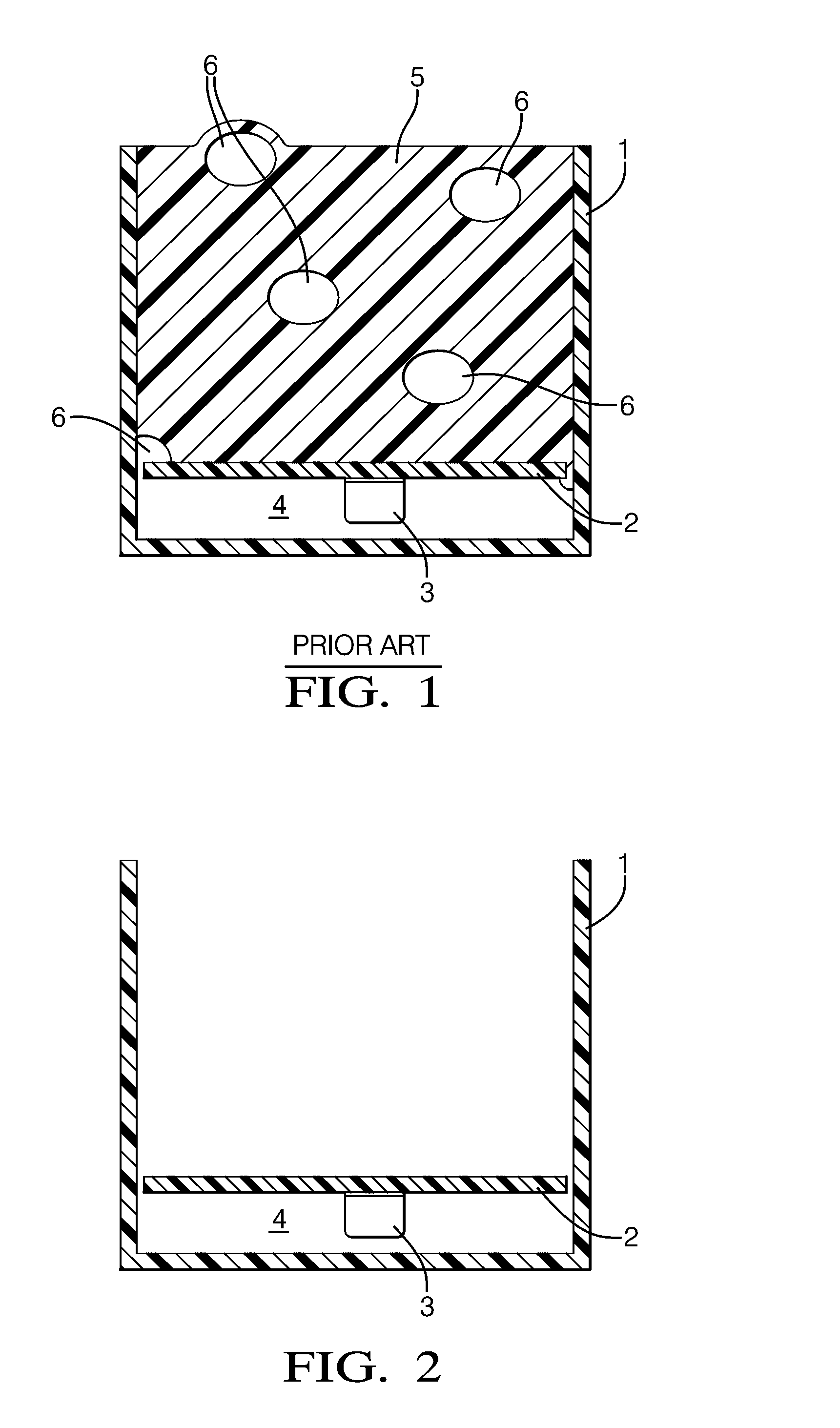
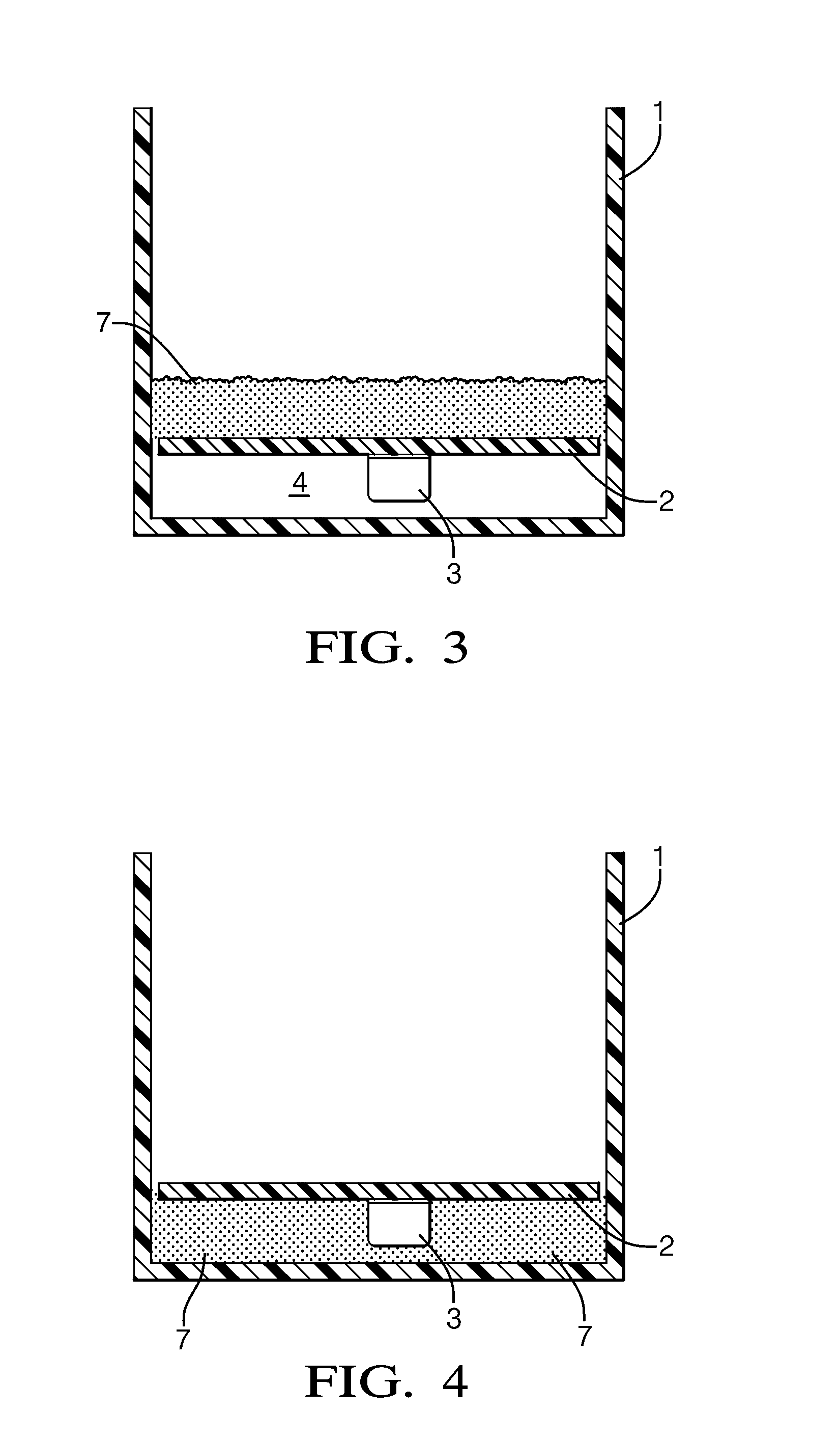
[0023]Referring now to FIGS. 2 -5, the method and assembly of the invention is illustrated in stages. In FIG. 2, there is shown the first stage of assembly where printed circuit board 2 having electronic components 3 mounted thereon is disposed in housing 1 with electronic components 3 disposed between circuit board 2 and housing 1, thereby forming spaces 4 between circuit board 2 and housing 1. In a non-limiting exemplary embodiment, the circuit board 2 may be affixed to housing 1 ...


PUM

PropertyMeasurementUnit
Temperatureaaaaaaaaaa
Lengthaaaaaaaaaa
Diameteraaaaaaaaaa

Abstract

A method of manufacturing an electronic component assembly is disclosed comprising disposing an electronic component in a housing such that there is at least one void space between the component and the housing, disposing non-conductive microspheres in the void space to substantially fill the void space, and disposing a fluid potting material in the housing and hardening or curing the potting material to pot the component in the housing. An assembly is also disclosed comprising a housing, an electronic component disposed in the housing such that there is at least one space between the component and the housing and the space is substantially filled with non-conductive microspheres, and a material that potting the first electronic component in the housing. The invention enables an electronic component in a housing with a space left between the housing to be potted with reduced formation of bubbles in the hardened potting material.

Description

BACKGROUND OF THE INVENTION[0001]In the manufacture of electronic components, the components are often disposed in a housing. In addition, the components are often seated or sealed in the housing with a potting material, usually a curable or hardenable polymer material such as an epoxy. Electronic components may be potted in a housing for a variety of reasons, such as to seal the electronic component against the environment in which the component is anticipated to operate, to enhance the attachment of the component to the housing, or to enhance the overall structural integrity of the housed component unit.[0002]In some circumstances, it may be desirable to completely fill a housing with potting material in order to fully encase the electronic component. Often times, however, it may be necessary that the housing is not completely filled with potting material. For example, the housing may contain electronic or other components in addition to the component desired to be potted that wil...

Claims


Application Information

Patent Timeline
IPC IPC(8): H01L23/28B29C70/70
CPCB29C39/006B29C39/10B29K2105/16B29K2105/165H01L21/54H01L2924/0002H01L21/56H01L2924/00
Inventor COVERS, ROBERTUS W.
Owner DELPHI TECH INC
Why Eureka
Try Eureka