

Area efficient through-hole connections
- Summary
- Abstract
- Description
- Claims
- Application Information
AI Technical Summary
Benefits of technology
Problems solved by technology
Method used
Image

Examples
Embodiment Construction
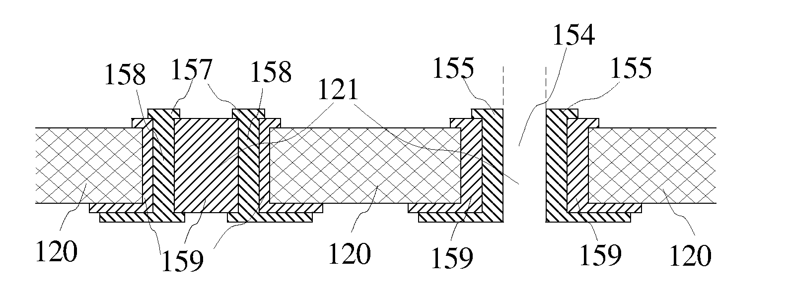
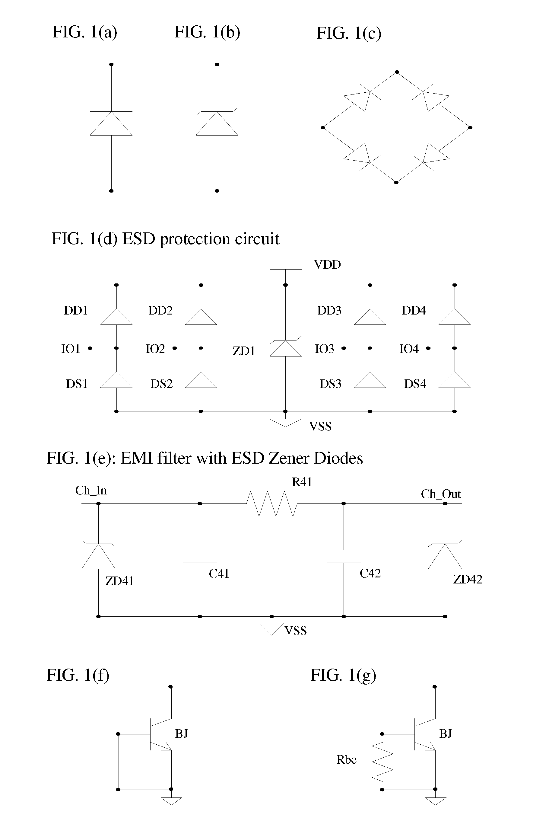
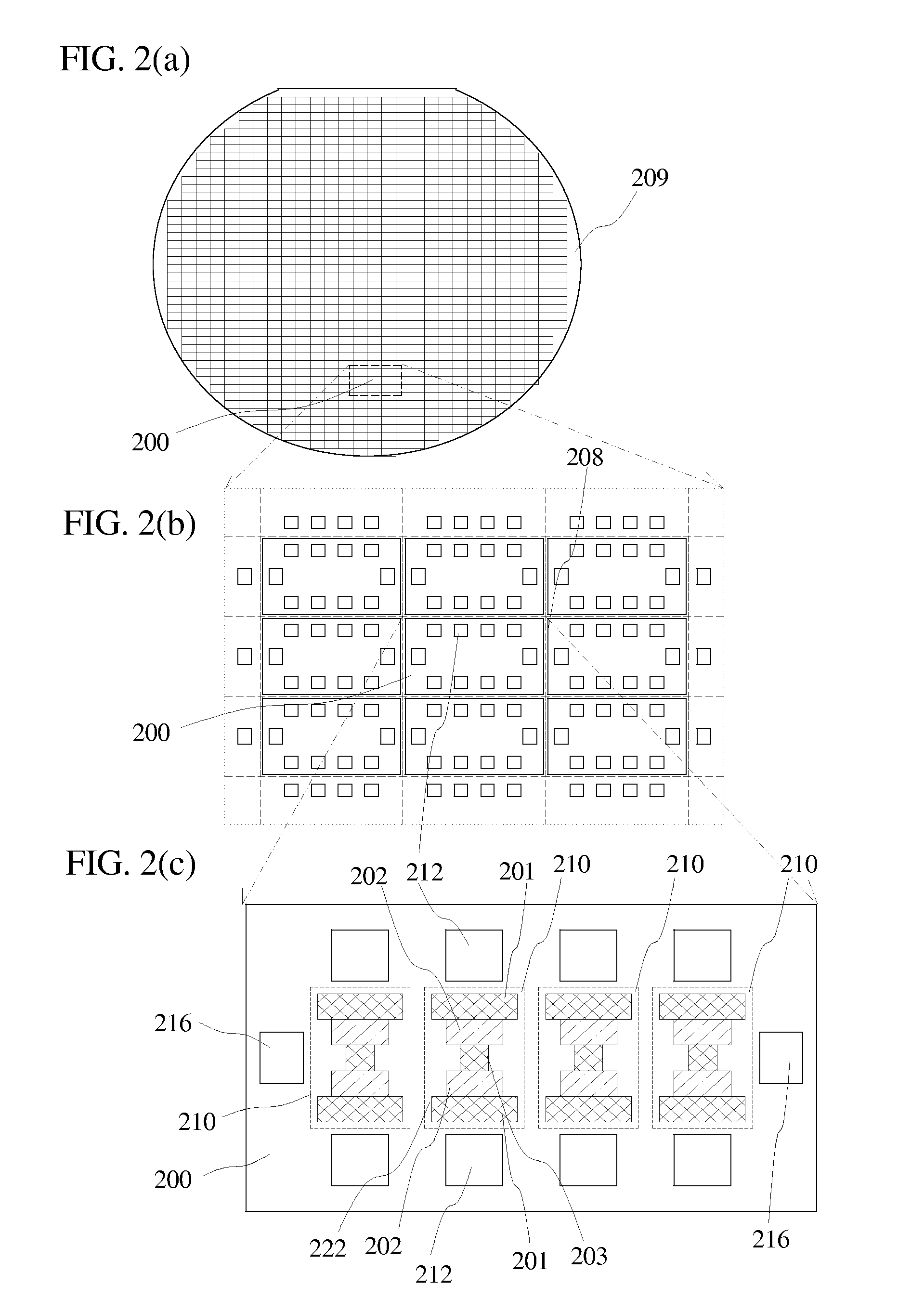
[0028]The primary objective of our preferred embodiment is, therefore, to reduce the area of surface mount package chips that comprise active electrical devices built on silicon substrate(s). The other objective of our preferred embodiment is to provide cost effective surface mount package chips. The other objective of our preferred embodiment is to reduce the parasitic inductance on the I / O connections of surface mount package chips. The other primary objective of our preferred embodiment is to reduce area occupied by through-hole conductors. Another objective of our preferred embodiment is to provide better control on the parasitic parameters of through-hole connections. These and other objectives are achieved by using side-wall conductor leads instead of bumping methods, and / or by using holes patterned in developed photo-resist materials.
[0029]While the novel features of the invention are set forth with particularly in the appended claims, our preferred embodiments, both as to or...
PUM
 Abstract
Description
Claims
Application Information