Method for forming fine pattern in semiconductor device

a technology of contact holes and semiconductor devices, which is applied in the direction of instruments, photomechanical devices, optics, etc., can solve the problems of increasing the likelihood of misalignment, complicating the overall process of forming a fine pattern, and difficulty in forming fine patterns that are finer than the maximum resolution of the apparatus, so as to achieve simplified process steps

Active Publication Date: 2011-05-26
SK HYNIX INC
View PDF4 Cites 384 Cited by
  • Summary
  • Abstract
  • Description
  • Claims
  • Application Information

AI Technical Summary

Benefits of technology

[0009]The present invention is directed to provide a novel method

Problems solved by technology

Since the maximum resolution of a photolithography apparatus is preset, it is difficult to form patterns that are finer than the maximum resolution of the apparatus.
In particularly, in order to form patterns having a pitch finer than the maximum resolution, a masking process is performed a plurality of times. This process complicates the overall

Method used


Image

  • Method for forming fine pattern in semiconductor device
  • Method for forming fine pattern in semiconductor device
  • Method for forming fine pattern in semiconductor device

Examples


Embodiment Construction

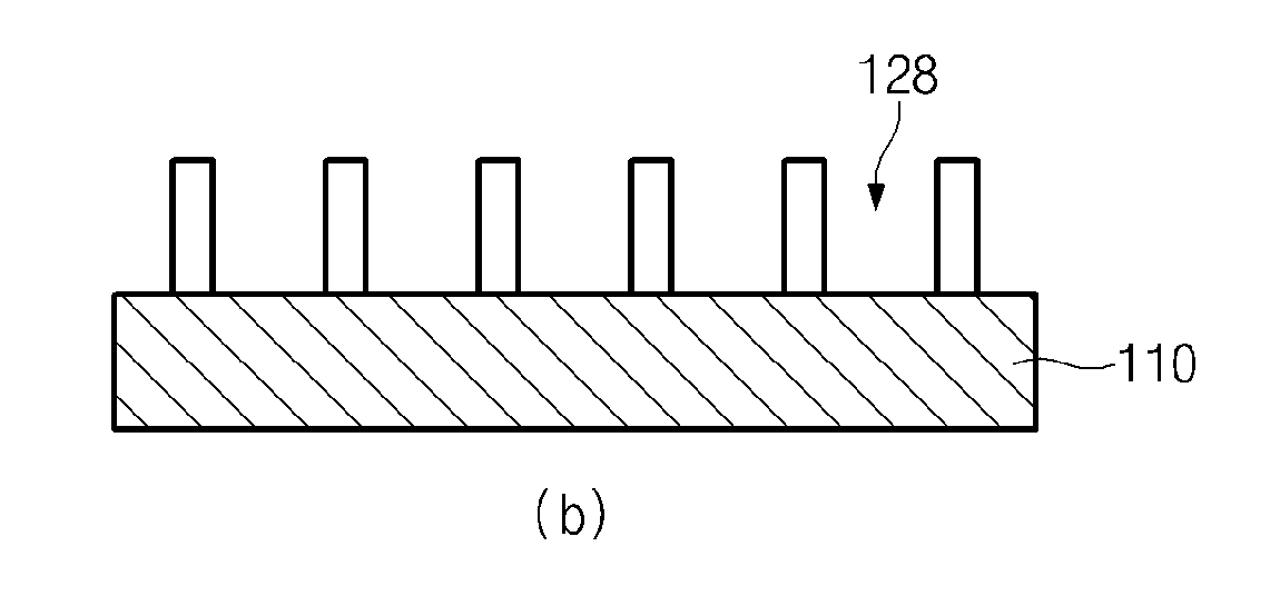
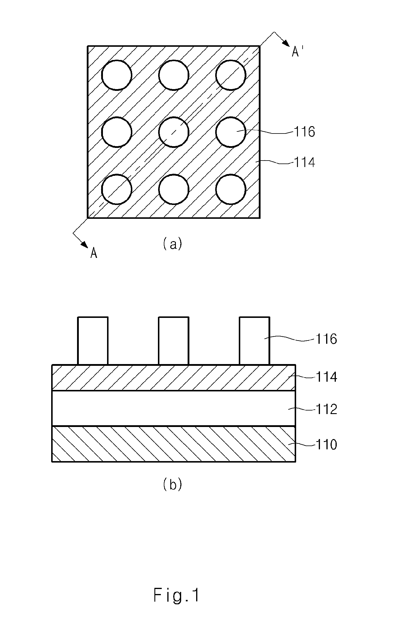
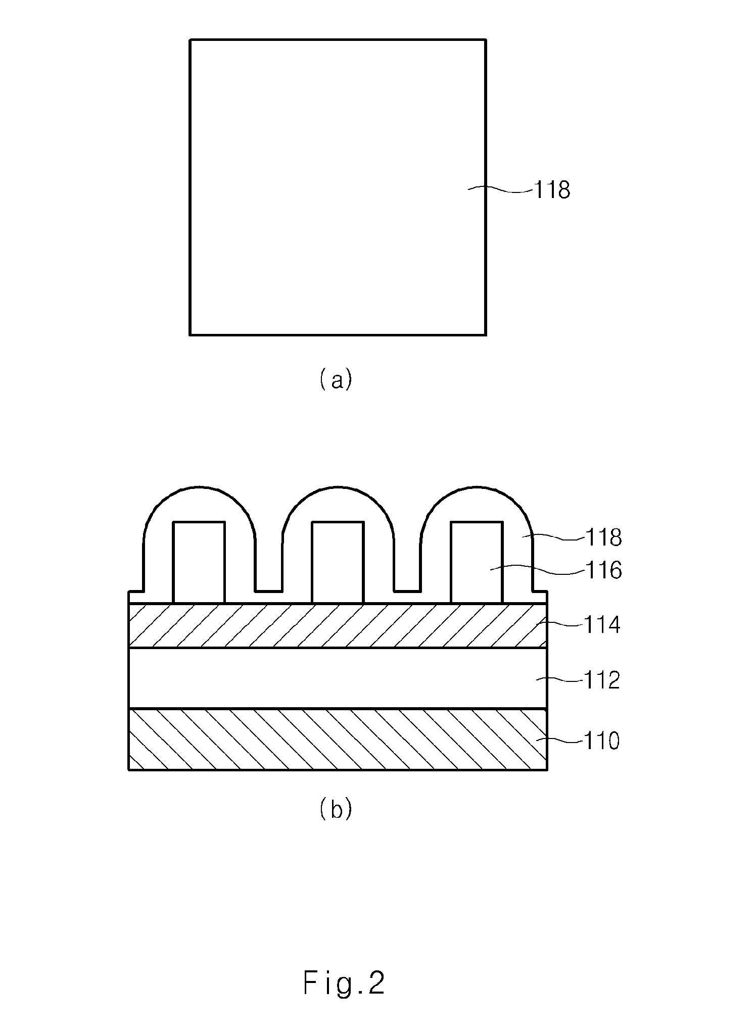
[0021]FIGS. 1 through 6 are views illustrating a method for forming a contact hole according to the present invention. FIGS. 1(a) through 6(a) are top views of FIGS. 1 through 6, and FIGS. 1(b) through 6(b) are cross-sectional views taken along the line A-A′ of FIG. 1.

[0022]First, referring to FIG. 1, a target etching layer (for example, an interlayer insulating film) 112, a hard mask layer 114 and a photoresist film (not shown) are formed over a semiconductor substrate. Next, a pillar patterning process is performed with a photolithography process using an exposure maskdefining a first contact hole region to form a photoresist film pattern 116. That is, the photoresist film pattern 116 includes pillar patterns formed in a pillar shape over the first contact hole region. The pillar pattern can be formed with a single patterning process using a single exposure mask or a double exposure process using line / space masks.

[0023]In addition, if a critical dimension (CD) of the pillar is too...


PUM

PropertyMeasurementUnit
Temperatureaaaaaaaaaa
Structureaaaaaaaaaa
Shapeaaaaaaaaaa

Abstract

A method for forming a contact hole of a semiconductor device according to the present invention forms a contact hole which is defined as a new contact hole region (a second contact hole region), between spacers as well as a contact hole defined within the spacer (a first contact hole region) by a spacer patterning technology (SPT). The present invention with this method can help to form a fine contact hole as a double patterning is used, even with one mask.

Description

CROSS-REFERENCE TO RELATED APPLICATION[0001]The present application claims priority to Korean patent application number 10-2009-0112535 filed on Nov. 20, 2009, which is incorporated by reference in its entirety.BACKGROUND OF THE INVENTION[0002]The present invention relates to a method for forming a contact hole of a semiconductor device. More particularly, the present invention relates to a method for forming a contact hole using a spacer patterning technology (SPT).[0003]Recently, as semiconductor devices become smaller and highly integrated, the whole chip area is increased in proportion to an increase in memory capacity. However, an area of a cell region in the semiconductor device, which contains patterns, is practically decreased.[0004]Thus, in order to form a large number of patterns in a limited cell region, a pitch size of patterns, for example, a critical dimension (CD) of a pattern or distance between two adjacent patterns becomes reduced.[0005]In addition, such fine patte...

Claims


Application Information

Patent Timeline
IPC IPC(8): H01L21/308H01L21/768
CPCH01L21/0337H01L21/76816H01L21/31144H01L21/0338G03F7/70433G03F7/7045
Inventor LEE, BYOUNG HOON
Owner SK HYNIX INC
Why Eureka
Try Eureka