Method for manufacturing an electronic assembly

Active Publication Date: 2011-06-16
ROBERT BOSCH GMBH
View PDF10 Cites 2 Cited by
  • Summary
  • Abstract
  • Description
  • Claims
  • Application Information

AI Technical Summary

Benefits of technology

[0023]Using the method according to the present invention it is possible to achieve a cost-effective wiring and encapsulation by using processes on many modules simultaneously and a reel-to-reel manufacture. It is moreover possible to process the electronic assembly further as a standard component for example. In the method according to the present invention, the electronic components are contacted during assembly. This requires fewer process steps than in the methods known from the related art.
[0024]Another advantage is that cost-effective plastics are used as the dielectric. Such plastics are kn

Problems solved by technology

A disadvantage of this assembly is that initially receptacles are cut into the circuit board substrate, into which the electronic components inserted.
This makes it very difficult to position the electronic components precisely.
Additional disadvantag

Method used


Image

  • Method for manufacturing an electronic assembly
  • Method for manufacturing an electronic assembly
  • Method for manufacturing an electronic assembly

Examples


Example

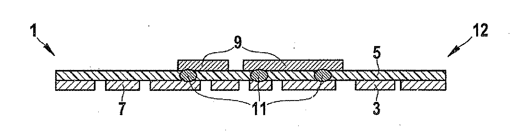
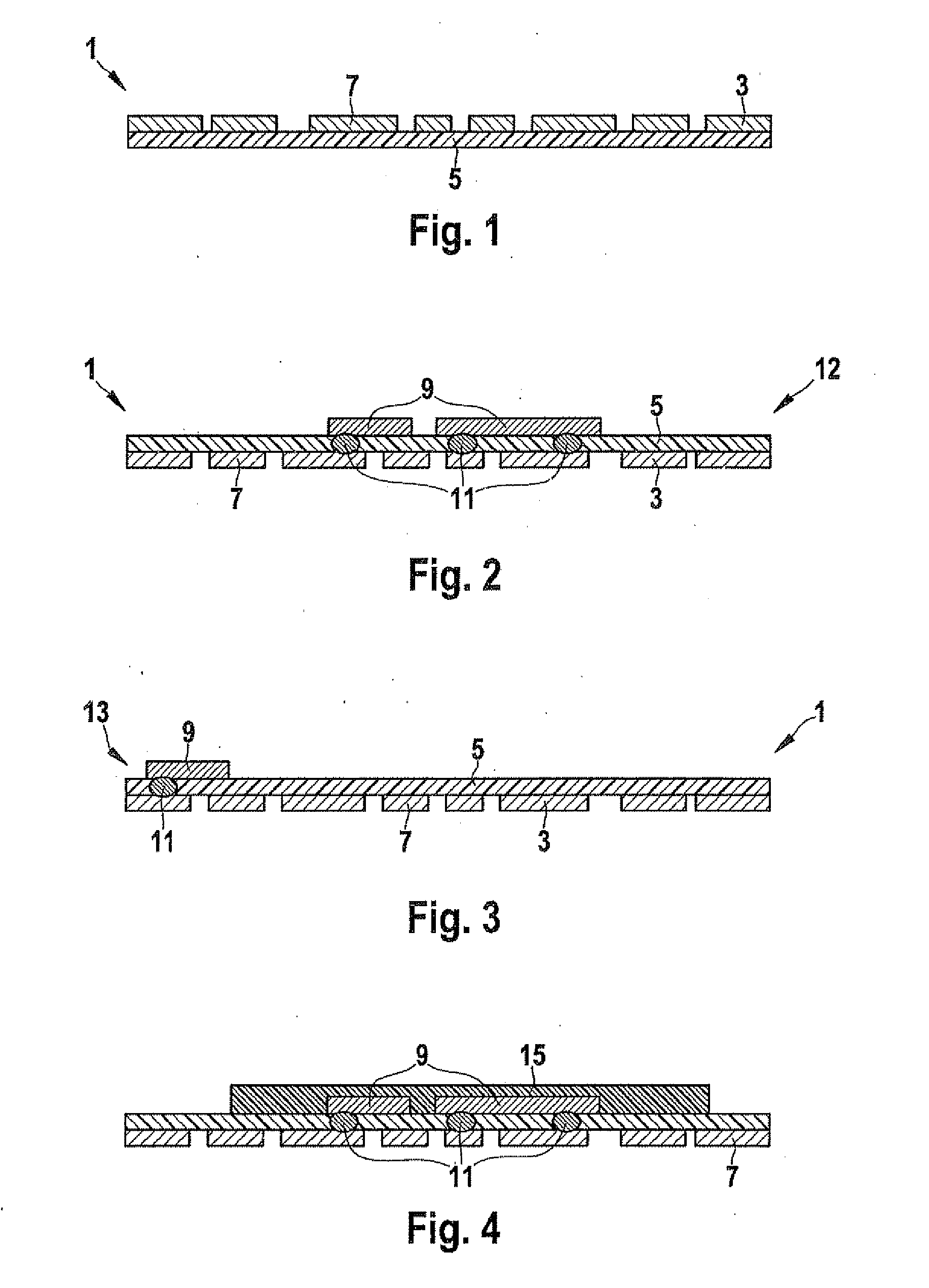
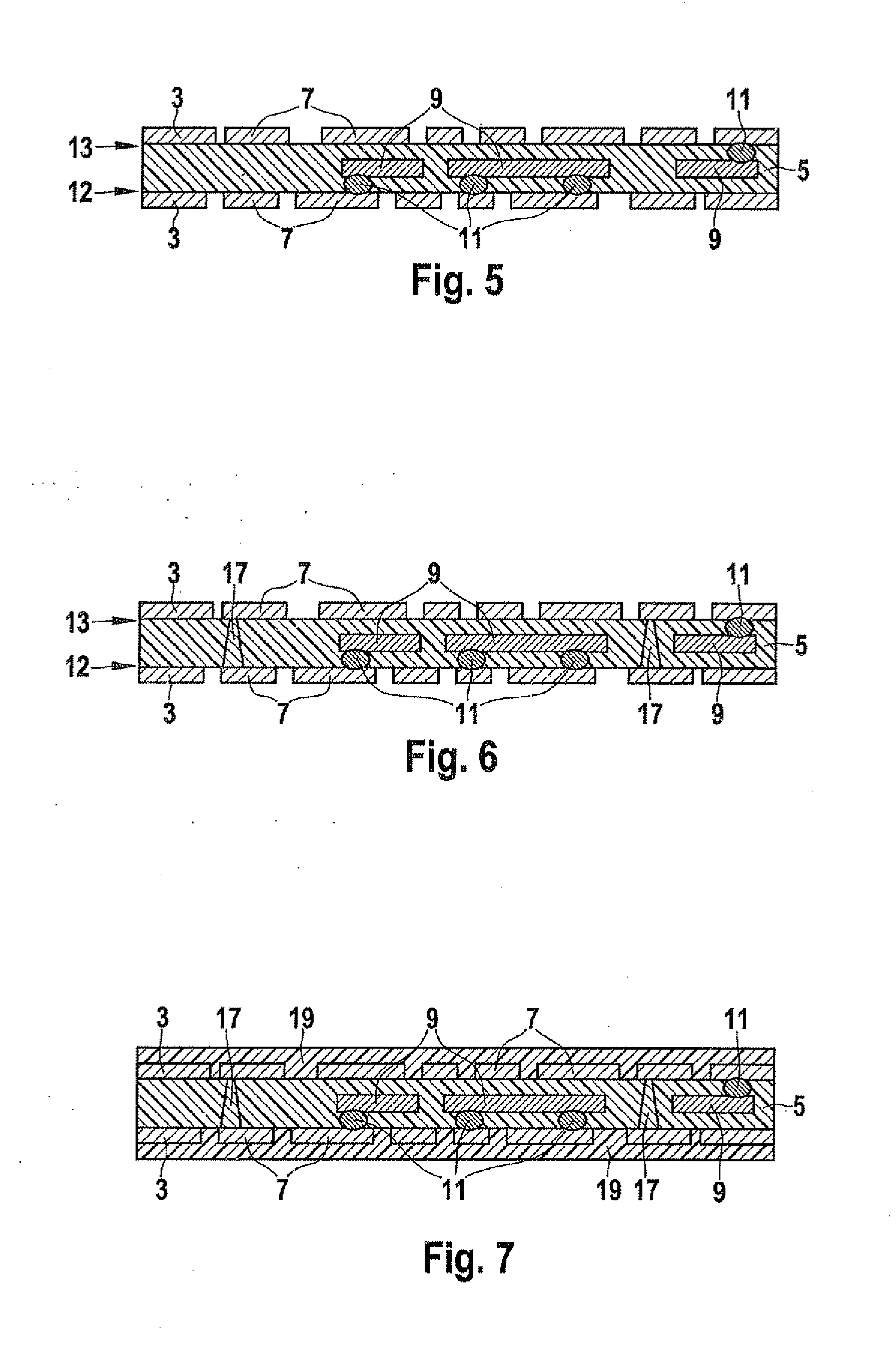
[0035]FIGS. 1 through 7 show individual method steps for manufacturing an electronic component developed in accordance with the exemplary embodiments and / or exemplary methods of the present invention.

[0036]In a first step, which is shown in FIG. 1, an electrically conductive foil 1 is patterned so as to develop a circuit trace structure. The patterning is performed only on an electrically conductive layer 3 of electrically conductive foil 1. In the specific embodiment shown here, electrically conductive layer 3 is applied on an electrically non-conductive layer 5. Electrically non-conductive layer 5 acts as a carrier layer and is not patterned. Electrically non-conductive layer 5 is a plastic layer for example. Particularly metals, for example copper or silver, are suitable as electrically conductive layer 3. Furthermore, gold, palladium or laminates, for example NiPdAu, are suitable as well. Electrically non-conductive layer 5 may be applied on electrically conductive layer 3 by la...


PUM

PropertyMeasurementUnit
Electrical conductivityaaaaaaaaaa
Electrical conductoraaaaaaaaaa
aaaaaaaaaa

Abstract

A method for manufacturing an electronic assembly, including at least one electronic component and a circuit trace structure, by which the at least one electronic component is contacted. In the method, a conductive foil is patterned in a first step to form the circuit trace structure. In a second operation, the circuit trace structure is equipped with the at least one electronic component. In a final operation, another foil is laminated onto the conductive foil equipped with the at least one electronic component on the side on which the conductive foil is equipped with the at least one electronic component.

Description

FIELD OF THE INVENTION[0001]The present invention relates to a method for manufacturing an electronic assembly, including at least one electronic component and a circuit trace structure, by which the at least one electronic component is contacted.BACKGROUND INFORMATION[0002]Electronic components used for manufacturing the electronic assembly are integrated circuits (IC) for example. These are accommodated in a substrate, for example in order to encapsulate them and to increase the surface area utilization on the electronic circuit carrier. This makes it possible to protect the electronic components. U.S. Pat. No. 6,512,182, for example, discusses cutting receptacles into a circuit board substrate, into which the electronic components are inserted. Once the electronic components have been inserted, the receptacles are filled, then smoothed and laminated over. Embedding the electronic components makes it possible to achieve a smooth surface of the electronic assembly.[0003]A disadvant...

Claims


Application Information

Patent Timeline
IPC IPC(8): H05K3/30
CPCH01L21/4825Y10T29/49126H01L23/5389H01L24/18H01L24/82H01L2221/68377H01L2224/16237H01L2224/18H01L2924/01029H01L2924/01033H01L2924/01046H01L2924/01047H01L2924/01079H01L2924/01082H01L2924/14H05K1/0284H05K1/186H05K1/189H05K3/0014H05K3/4038H05K2201/0305H05K2201/0355H05K2201/10674H05K2203/302H01L2924/01005H01L2924/01006H01L2924/01068H01L2924/014H01L2924/07802H01L23/5387Y10T29/49165Y10T29/4913H01L2924/00H01L2924/181H01L2224/05573H01L2224/05568H01L2924/00014H01L24/96H01L2224/05599
Inventor SCHAAF, ULRICHKUGLER, ANDREAS
Owner ROBERT BOSCH GMBH
Why Eureka
Try Eureka