CMOS switch for use in radio frequency switching and isolation enhancement method

a technology of radio frequency switching and switch, applied in the field of switch, can solve the problems of degrading the isolation properties of the switch, increasing the insertion loss, etc., and achieve the effect of improving the isolation properties and enhancing the isolation of the switch

Inactive Publication Date: 2011-06-16
ELECTRONICS & TELECOMM RES INST
View PDF6 Cites 11 Cited by
  • Summary
  • Abstract
  • Description
  • Claims
  • Application Information

AI Technical Summary

Benefits of technology

[0010]Embodiments of the present invention provide a CMOS switch which has improved isolation properties, and a method for enhancing a switching isolation.
[0011]Embodiments of the present invention also provide a CMOS switch for use in RF switching which is simply structured and has excellent operating properties at the MF or higher band.
[0012]Embodiments of the present invention also provide a CMOS switch for use in RF switching capable of substantially preventing a leakage current at a switching operation.
[0016]In other embodiments of the present invention, CMOS switches for use in RF switching include: a serial switching unit including first and second CMOS switches connected between two output terminals and constructing a SPDT switch; a switching isolation unit for allowing an unselected output terminal of the two output terminals to be electrically isolated from a common input terminal when the serial switching unit operates; a first isolation enhancement unit connected in parallel to the first and the second CMOS switches between the two output terminals, and enhancing a switching isolation of the serial switching unit by forming a parallel resonance circuit with a parasitic capacitor of the serial switching unit; and a second isolation enhancement unit connected between the common input terminal and a ground, and enhancing the switching isolation and input matching properties of the serial switching unit.
[0021]In even other embodiments of the present invention, CMOS switches for use in RF switching include: a serial switching unit including a first CMOS switch and a second CMOS switch, wherein the first CMOS switch is connected between a common input terminal and a first output terminal for switching the common input terminal to the first output terminal in response to a first control signal, and the second CMOS switch is connected between the common input terminal and a second output terminal for switching the common input terminal to the second output terminal in response to a second control signal; a switching isolation unit including a first shunt element and a second shunt element, wherein the first shunt element allows the second output terminal to be electrically isolated from the common input terminal in response to the first control signal when the first CMOS switch operates, and the second shunt element allows the first output terminal to be electrically isolated from the common input terminal in response to the second control signal when the second CMOS switch operates; a first isolation enhancement unit connected in parallel to the first and the second CMOS switches between the first and the second output terminals, and enhancing a switching isolation of the serial switching unit by forming a parallel resonance circuit together with a parasitic capacitor of the serial switching unit; and a second isolation enhancement unit connected between the common input terminal and a ground enhancing the switching isolation and input matching properties of the serial switching unit.

Problems solved by technology

However, as the operating frequency of the signal increases, the insertion loss increases, and particularly the isolation properties of the switch are degraded due to a parasitic capacitance.

Method used


Image

  • CMOS switch for use in radio frequency switching and isolation enhancement method
  • CMOS switch for use in radio frequency switching and isolation enhancement method
  • CMOS switch for use in radio frequency switching and isolation enhancement method

Examples


first embodiment

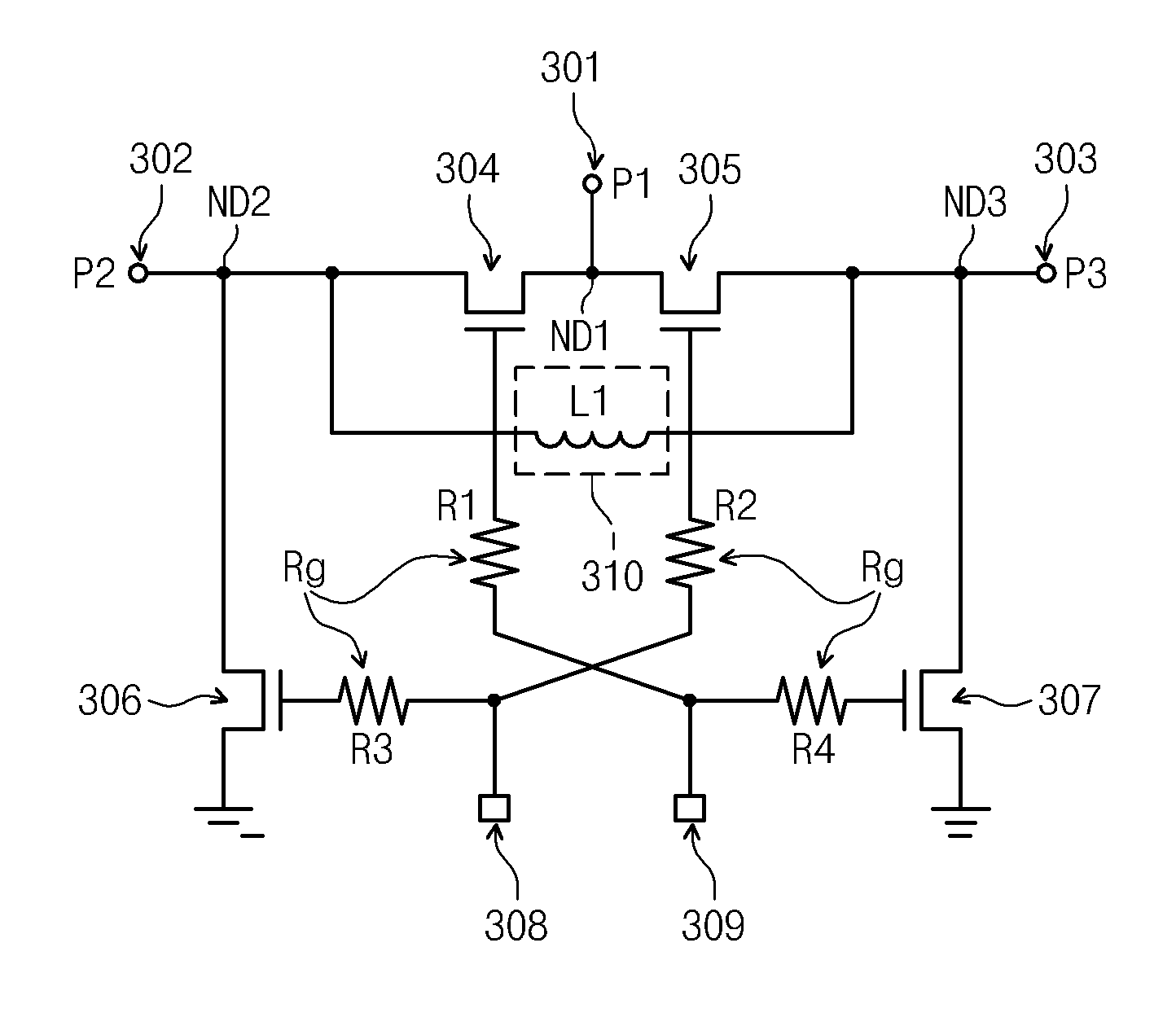
[0037]FIG. 3 is a circuit diagram of a CMOS switch for use in RF switching according to the present invention.

[0038]It will be explained that the switching isolation properties are improved by connecting an inductor element in parallel to a switching element in the case of the first embodiment illustrated in FIG. 3. FIG. 3 illustrates an exemplary embodiment of a CMOS RF switch, and it will be understood that the embodiment may be suitable for a CMOS SPDT switch used in an MF band. The CMOS RF switch may be fabricated by using various semiconductor manufacturing processes including, e.g., a 0.25 μm process.

[0039]Referring to FIG. 3, unlike FIG. 1, an isolation enhancement unit 310 is connected in parallel to first and second CMOS switches 304 and 305 between first and second output terminals P2 and P3. The isolation enhancement unit 310, which may be embodied with an inductor L1, forms a parallel resonance circuit with a parasitic capacitor generated due to the first and the second ...

second embodiment

[0046]A second embodiment will now be described referring to FIG. 4.

[0047]FIG. 4 is a circuit diagram of a CMOS switch for use in RF switching according to the second embodiment of the present invention.

[0048]Referring to FIG. 4, a serial switching unit includes a first CMOS switch 404 and a second CMOS switch 405. The first CMOS switch 404 is connected between a common input terminal 401 and a first output terminal 402. The first CMOS switch 404 switches the common input terminal 401 to the first output terminal 402 in response to a first control signal applied to a first control terminal 409. The second CMOS switch 405 is connected between the common input terminal 401 and a second output terminal 403. The second CMOS switch 405 switches the common input terminal 401 to the second output terminal 403 in response to a second control signal applied to a second control terminal 408.

[0049]A switching isolation unit includes a first shunt element 407 and a second shunt element 406. The...


PUM


Abstract

Provided is a CMOS switch for use in RF switching having improved isolation properties. The CMOS switch includes a serial switching unit having first and second CMOS switches, a switching isolation unit for allowing an unselected output terminal of two output terminals to be electrically isolated from a common input terminal when the serial switching unit operates and an isolation enhancement unit. The isolation enhancement unit is connected in parallel to the first and the second CMOS switches between the two output terminals forming a parallel resonance circuit together with a parasitic capacitor of the serial switching unit. The CMOS switch for use in RF switching according to the present invention has a simple circuit structure and excellent operating properties at the MF or higher band. Also, the CMOS switch having high isolation properties is realized.

Description

CROSS-REFERENCE TO RELATED APPLICATIONS[0001]This U.S. non-provisional patent application claims priority under 35 U.S.C. §119 of Korean Patent Application No. 10-2009-0125605, filed on Dec. 16, 2009, the entire contents of which are hereby incorporated by reference.BACKGROUND OF THE INVENTION[0002]The present invention disclosed herein relates to a switch used for controlling the path of a Radio Frequency (RF) signal in a Microwave Frequency (MF) component and system, and more particularly, to a Complementary Metal Oxide Semiconductor (CMOS) switch operating in the RF band such as the MF band.[0003]The development of the Integrated Circuit (IC) technology has greatly contributed to the advancement of the wireless communication industry over the decades. Due to the development of the wireless communication industry, RF components such as low-noise amplifiers, oscillators, high-output amplifiers and switches, which are fabricated using the IC technology, particularly the CMOS technol...

Claims


Application Information

Patent Timeline
Patent Type & Authority Applications(United States)
IPC IPC(8): H03K17/687
CPCH03K17/005H04B1/48H03K17/693H03K17/687
Inventor SHIN, DONG HWANYOM, IN BOK
Owner ELECTRONICS & TELECOMM RES INST
Why Eureka
Try Eureka