Testing embedded memories in an integrated circuit

a technology of embedded memory and integrated circuit, which is applied in the direction of error detection/correction, program control, instruments, etc., can solve the problems of long test time, permanent penalty for memory performance, and plurality of multiplexers, so as to reduce the overhead of hardware and minimize hardware.

Active Publication Date: 2011-06-16
SIEMENS PROD LIFECYCLE MANAGEMENT SOFTWARE INC
View PDF19 Cites 6 Cited by
  • Summary
  • Abstract
  • Description
  • Claims
  • Application Information

AI Technical Summary

Benefits of technology

Similarly, in some embodiments, the act of synthesizing includes minimizing the hardware by identifying two or more of the control points that can be coupled to a single respective output of the memory-test controller. For instance, the act of synthesizing might comprise inserting a fan-out from a single respective output of the memory-test controller to control two or more of the control points. In such an embodiment, placement of the fan-out can be delayed in order to reduce the area overhead of the hardware.

Problems solved by technology

This method, however, can involve long test times because a large number of shifts are necessary to load the appropriate test values (each shift consumes one clock cycle).
A major drawback of conventional MBIST circuits, however, is that a plurality of multiplexers are placed before the inputs of the memory-under-test in order to input the test vectors.
These multiplexers produce a delay in the system paths to the memory inputs, and thus create a permanent penalty in memory performance.
Additionally, when the memory is tested at-speed, delay faults in the memory and delay faults in the logic around the memory may escape from being detected.
Consequently, certain delay faults cannot be detected by the conventional MBIST architecture.
Similar problems are experienced along the output paths of the memories.

Method used


Image

  • Testing embedded memories in an integrated circuit
  • Testing embedded memories in an integrated circuit
  • Testing embedded memories in an integrated circuit

Examples


Embodiment Construction

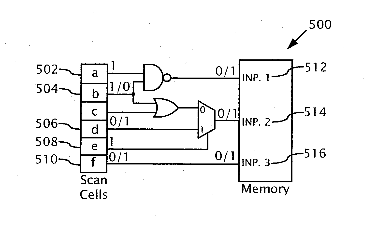
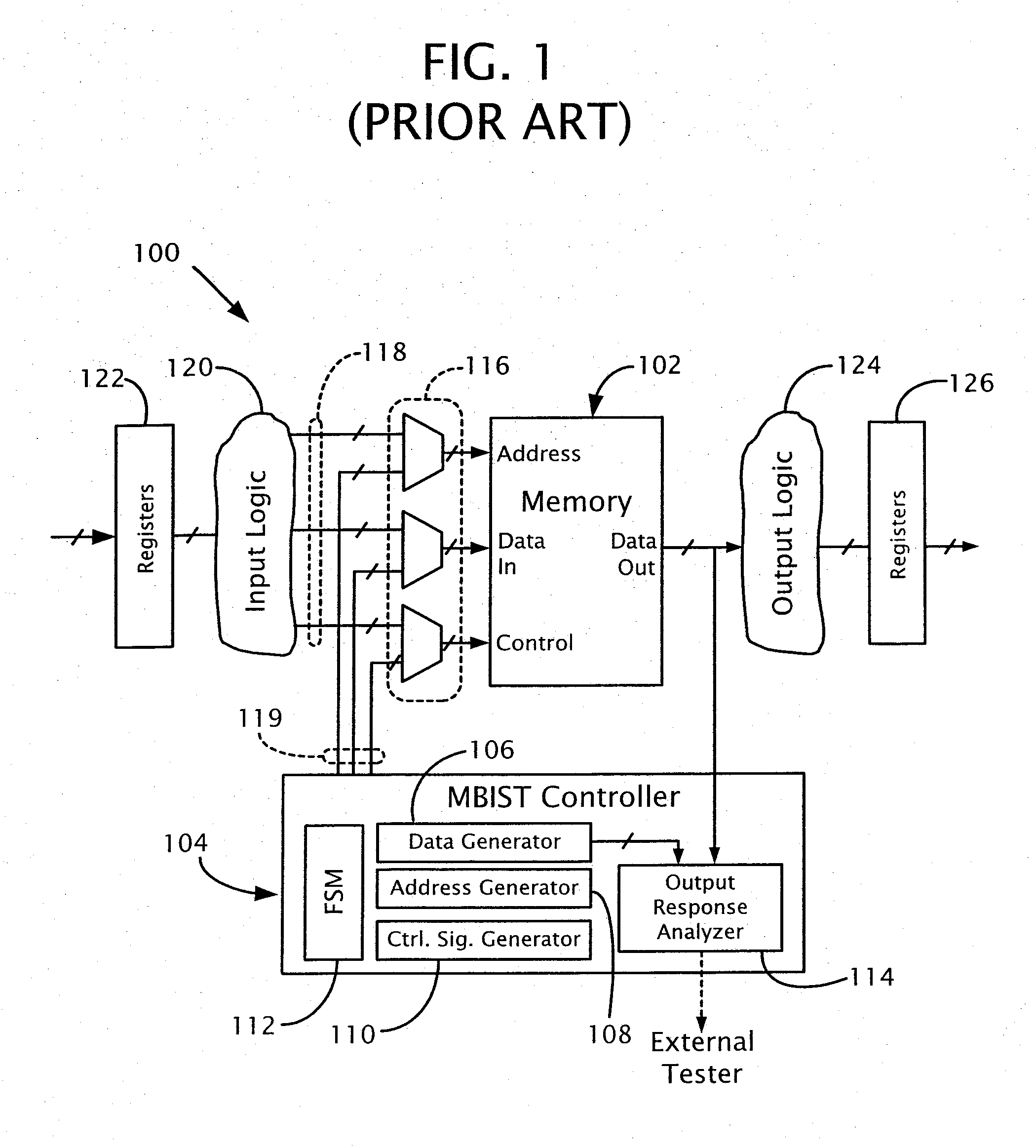
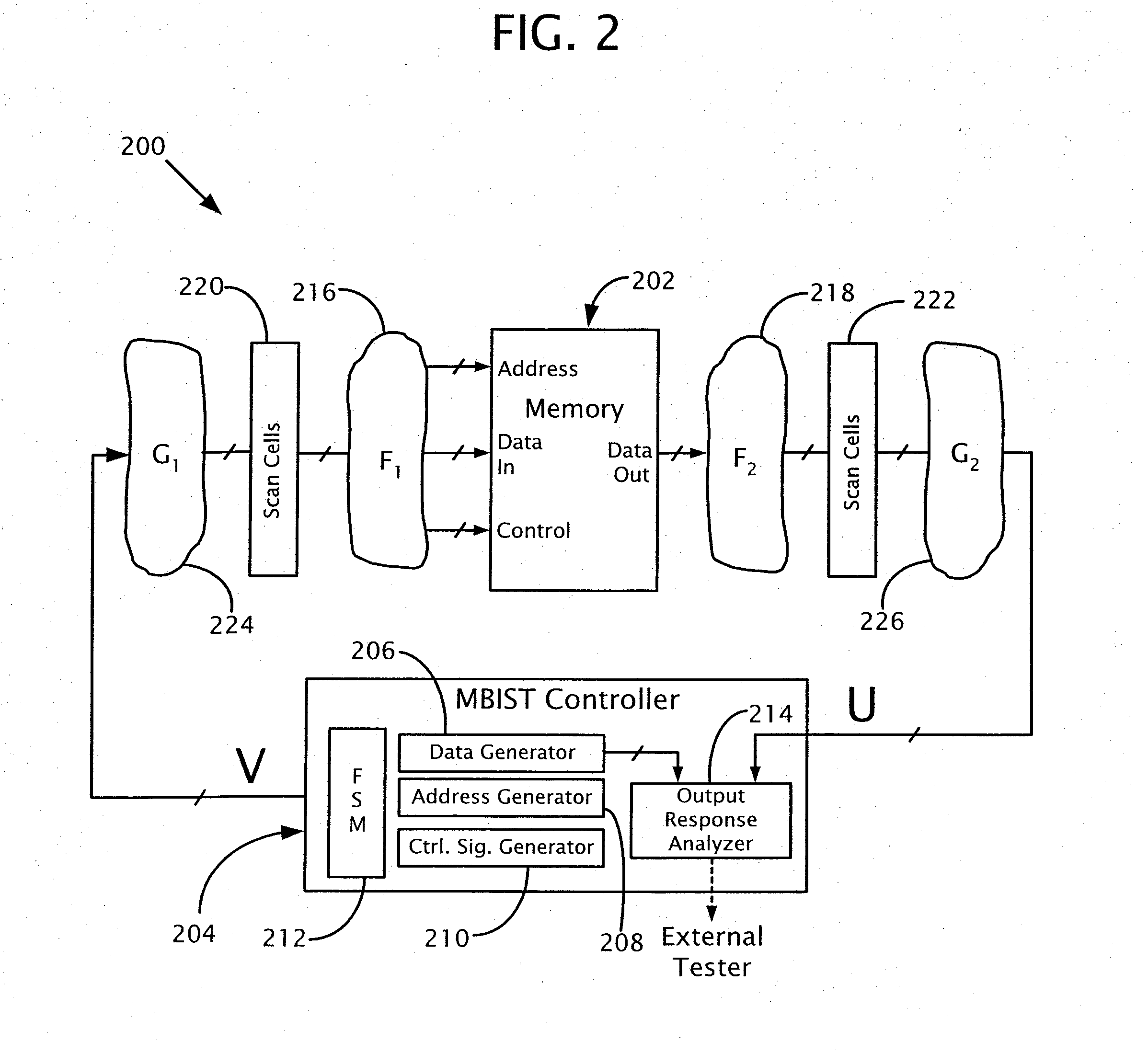
Disclosed below are representative embodiments of methods and apparatus for testing embedded memories in an integrated circuit using built-in self-test (BIST) hardware. Such hardware is collectively referred to as “memory BIST” or “MBIST.” Desirably, testing is performed at-speed and with less or none of the unnecessary delay that is introduced by conventional MBIST circuits. The disclosed methods and apparatus should not be construed as limiting in any way. Instead, the present disclosure is directed toward novel and nonobvious features and aspects of the various disclosed embodiments, alone and in various combinations and subcombinations with one another. Moreover, the methods and apparatus are not limited to any specific aspect or feature or combinations thereof, nor do the disclosed methods and apparatus require that any one or more specific advantages be present or problems be solved.

Although the operations of some of the disclosed methods and apparatus are described in a parti...


PUM


Abstract

Various new and non-obvious apparatus and methods for testing embedded memories in an integrated circuit are disclosed. One of the disclosed embodiments is an apparatus for testing an embedded memory in an integrated circuit. This exemplary embodiment comprises input logic that includes one or more memory-input paths coupled to respective memory inputs of the embedded memory, a memory built-in self-test (MBIST) controller, and at least one scan cell coupled between the input logic and the MBIST controller. The scan cell of this embodiment is selectively operable in a memory-test mode and a system mode. In memory-test mode, the scan cell can apply memory-test data to the memory inputs along the memory-input paths of the integrated circuit. Any of the disclosed apparatus can be designed, simulated, and / or verified (and any of the disclosed methods can be performed) in a computer-executed application, such as an electronic-design-automation (“EDA”) software tool.

Description

TECHNICAL FIELD This application relates to the testing of embedded memories in an integrated circuit using hardware that is built into the chip.BACKGROUND In modern integrated-circuit design, embedded memories occupy a large area of a chip. In microprocessors, for example, embedded memories can occupy more than 30% of the chip area, and in a system-on-a-chip (SoC), they can exceed 60%. The memory array is typically the densest physical structure on the chip and is usually made from the smallest geometry process features available.To test an embedded memory, a variety of methods have been developed. One known method utilizes unmodified scan cells to load test vectors from an external tester and to capture the output responses from the memory. This method, however, can involve long test times because a large number of shifts are necessary to load the appropriate test values (each shift consumes one clock cycle). Thus, this method is most useful for smaller memories where the number o...

Claims


Application Information

Patent Timeline
Patent Type & Authority Applications(United States)
IPC IPC(8): G06F17/50G11C29/48
CPCG11C29/1201G11C29/48G11C2029/3202G11C2029/0405G11C2029/0401
Inventor ROSS, DON E.DU, XIAOGANGCHENG, WU-TUNGRAYHAWK, JOSEPH C.
Owner SIEMENS PROD LIFECYCLE MANAGEMENT SOFTWARE INC
Why Eureka
Try Eureka