Dual layer gate dielectrics for non-silicon semiconductor devices

a technology of non-silicon semiconductor devices and dielectrics, which is applied in the direction of semiconductor devices, basic electric elements, electrical appliances, etc., can solve the problems of preventing widespread adoption of iii-v semiconductor transistor devices and forming good quality gates

Inactive Publication Date: 2011-06-23
INTEL CORP
View PDF1 Cites 38 Cited by
  • Summary
  • Abstract
  • Description
  • Claims
  • Application Information

AI Technical Summary

Problems solved by technology

Such non-silicon devices offer the promise of exceptionally high carrier mobility in the transistor channels due to low effective carrier mass.
However, as those in the art will appreciate, the inability...

Method used


Image

  • Dual layer gate dielectrics for non-silicon semiconductor devices
  • Dual layer gate dielectrics for non-silicon semiconductor devices
  • Dual layer gate dielectrics for non-silicon semiconductor devices

Examples


Embodiment Construction

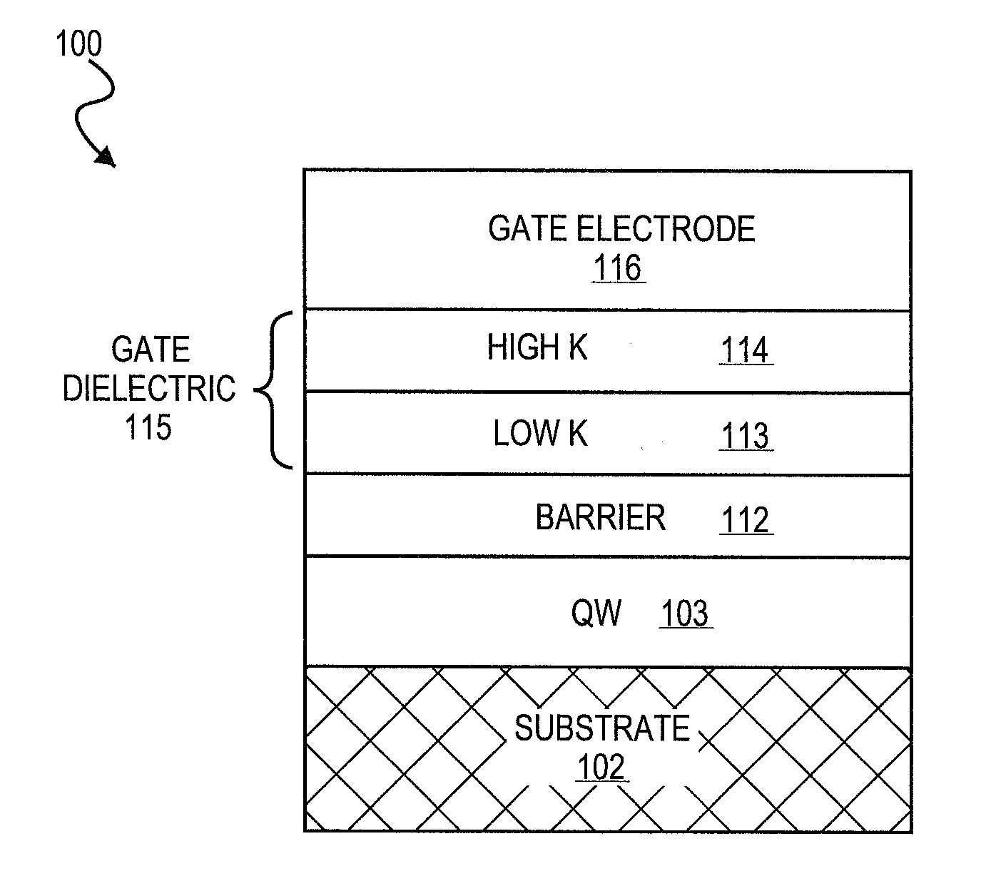
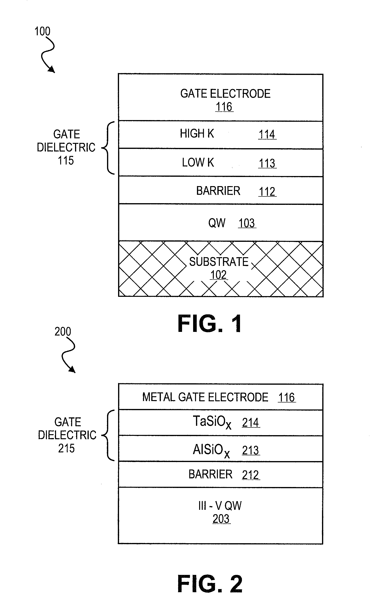
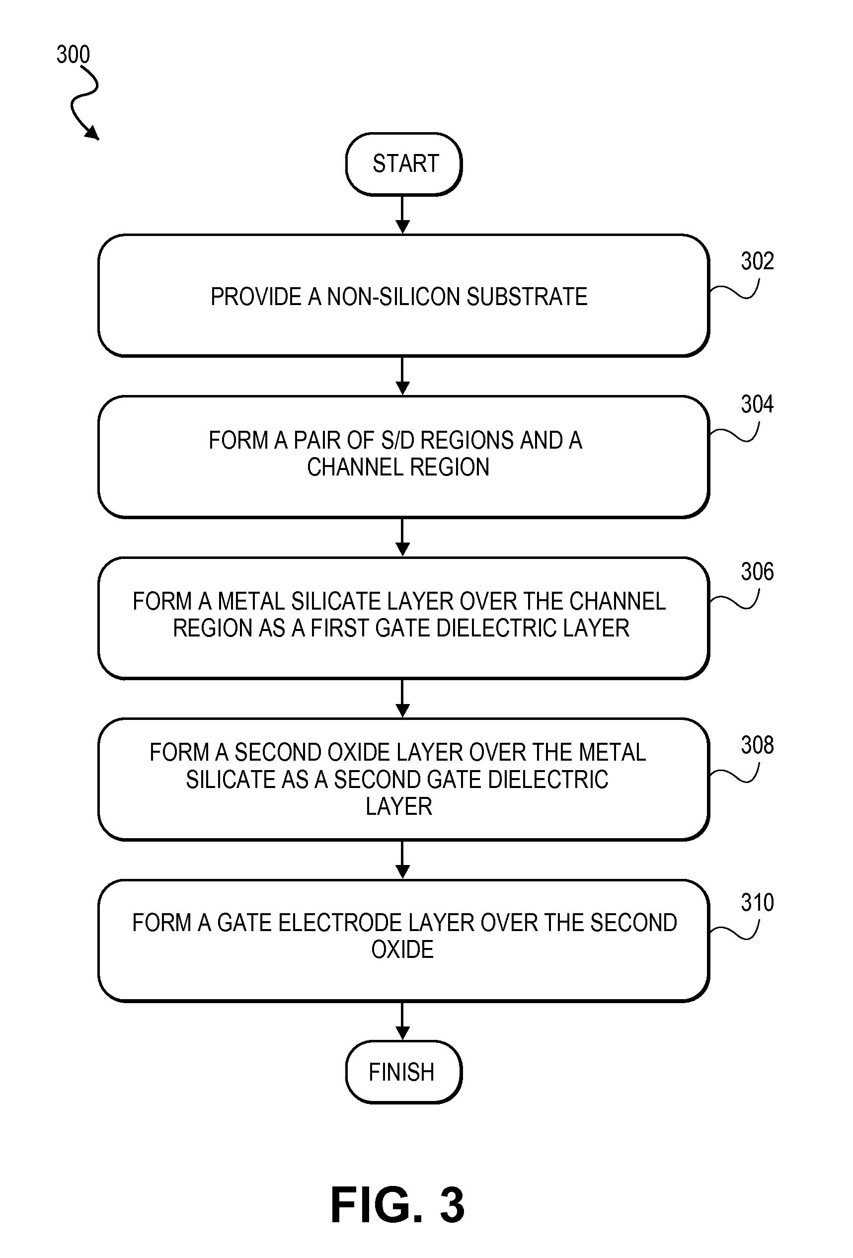
Non-silicon devices employing a gate dielectric stack including at least a first and second gate dielectric are described. In the following description, numerous specific details are set forth, such as material compositions and film characteristics, in order to provide a thorough understanding of embodiments of the present invention. It will be apparent to one skilled in the art that embodiments of the present invention may be practiced without these specific details. In other instances, well-known features, such as patterning processes, are not described in detail in order to not unnecessarily obscure embodiments of the present invention. Furthermore, it is to be understood that the various embodiments shown in the Figures are illustrative representations and are not necessarily drawn to scale.

The terms “over,”“under,”“between,” and “on” as used herein refer to a relative position of one media layer with respect to other layers. As such, for example, one layer disposed over or unde...


PUM


Abstract

Non-silicon metal-insulator-semiconductor (MIS) devices and methods of forming the same. The non-silicon MIS device includes a gate dielectric stack which comprises at least two layers of non-native oxide or nitride material. The first material layer of the gate dielectric forms an interface with the non-silicon semiconductor surface and has a lower dielectric constant than a second material layer of the gate dielectric. In an embodiment, a dual layer including a first metal silicate layer and a second oxide layer provides both a good quality oxide-semiconductor interface and a high effective gate dielectric constant.

Description

TECHNICAL FIELDEmbodiments of the invention are in the field of Semiconductor Devices and, more particularly, transistors formed of non-silicon semiconductor materials.BACKGROUNDFor the past several decades, the scaling of features in integrated circuits has been a driving force behind an ever-growing semiconductor industry. Scaling to smaller and smaller features enables increased densities of functional units on the limited real estate of semiconductor chips. For example, shrinking transistor size allows for the incorporation of an increased number of memory devices on a chip, lending to the fabrication of products with increased capacity.Recently, research on non-silicon devices like high electron mobility transistors (HEMT) employing quantum-well field effect transistors (QWFET) has increased. Quantum-well devices are typically formed in epitaxially grown semiconductor hetero-structures, such as in compound semiconductor materials like III-V systems. Such non-silicon devices off...

Claims


Application Information

Patent Timeline
IPC IPC(8): H01L29/78H01L29/12H01L21/336
CPCH01L29/2003H01L29/513H01L29/7786H01L29/66462H01L29/66431
Inventor DEWEY, GILBERTRADOSAVLJEVIC, MARKOPILLARISETTY, RAVICHAU, ROBERT S.
Owner INTEL CORP
Why Eureka
Try Eureka