
Array substrate of display device

a display device and substrate technology, applied in the field of display devices, can solve the problems of difficult to implement a driving circuit that operates at high speed on account of low electron mobility, high electron mobility, and non-uniform threshold voltage, and achieve the effect of easy to achieve desired capacitan

Inactive Publication Date: 2011-06-23
SAMSUNG DISPLAY CO LTD
View PDF24 Cites 74 Cited by
  • Summary
  • Abstract
  • Description
  • Claims
  • Application Information

AI Technical Summary

Benefits of technology

[0010]Non-limiting example embodiments of the present invention provide an array substrate of a display device capable of easily achieving desired capacitance from a limited area.
[0017]According to non-limiting example embodiments of the present invention, in an array substrate of a display device using poly-silicon, it is possible to reduce the area that is occupied by a storage capacitor in a pixel region and achieve high luminance by increasing the aperture ratio, by providing a structure and method of increasing storage capacitance to the same area.

Problems solved by technology

When the semiconductor layer is formed using amorphous silicon, it is difficult to implement a driving circuit that operates at high speed on account of low electron mobility.
On the other hand, when the semiconductor layer is formed using poly-silicon, a threshold voltage becomes non-uniform due to a polycrystalline nature of the semiconductor layer, although electron mobility is high.
However, the increased overlap area reduces the aperture ratio of the pixel corresponding to the area that the upper storage electrode and the lower storage electrode occupy.

Method used


Image

  • Array substrate of display device
  • Array substrate of display device
  • Array substrate of display device

Examples


Embodiment Construction

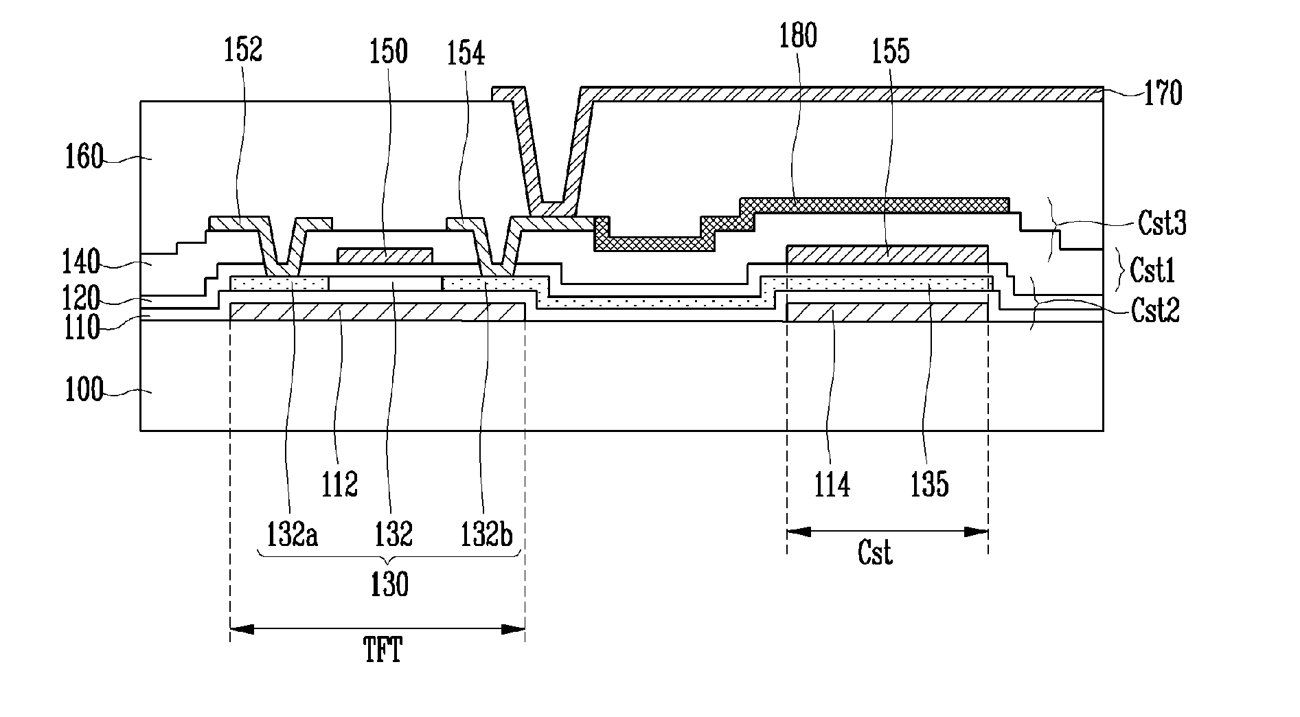
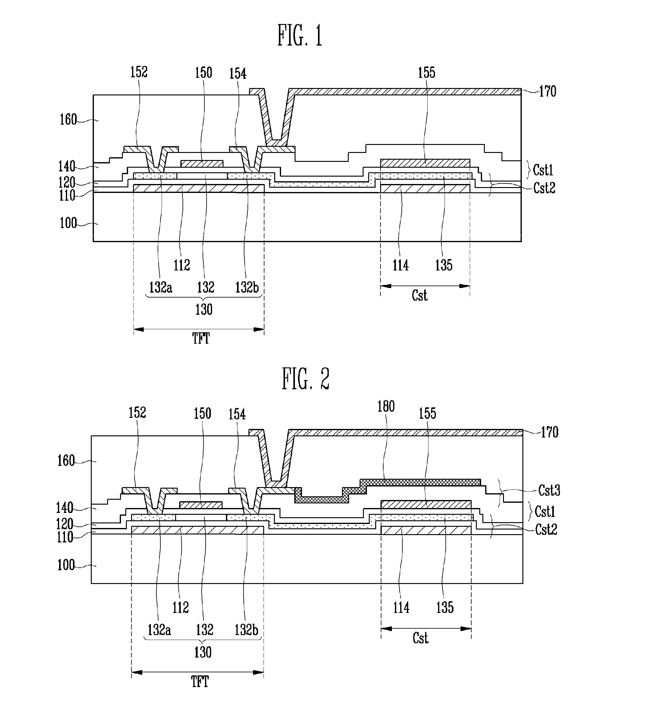
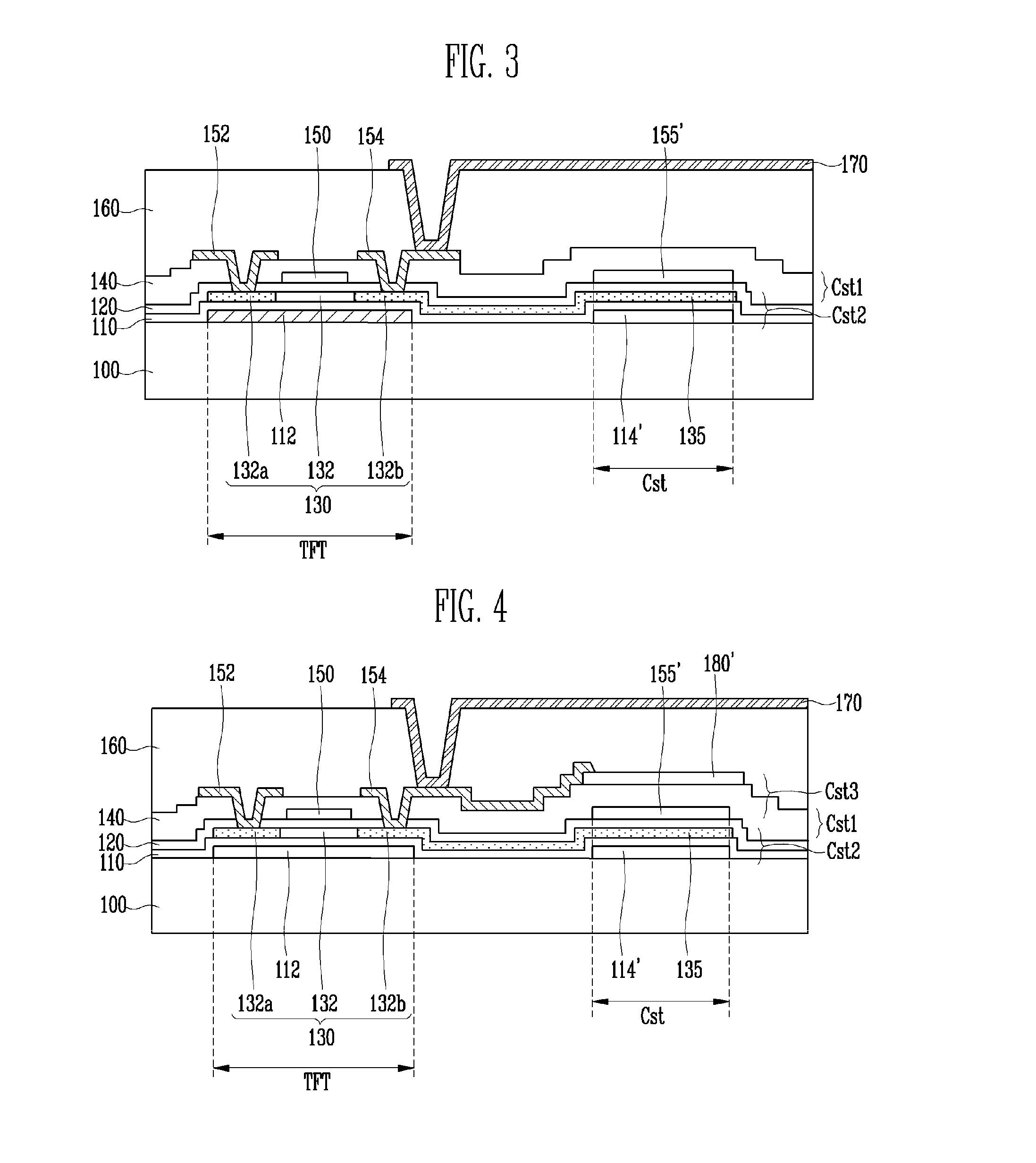
[0026]Reference will now be made in detail to the present non-limiting example embodiments of the present invention, examples of which are illustrated in the accompanying drawings, wherein like reference numerals refer to the like elements throughout. The non-limiting example embodiments are described below in order to explain the present invention by referring to the figures.

[0027]As referred to herein, it is to be understood that when it is stated that one film, element or layer is “formed on” or “located on” a second layer or film, the first layer, element or film may be formed or located directly on the second layer, element or film or there may be intervening layers, elements or films between the first layer, element or film and the second layer, element or film. Furthermore, as used herein, the term “formed on” is used with the same meaning as “located on” or “located on” and is not meant to be limiting regarding any particular fabrication process. Additionally, some of the el...


PUM


Abstract

An array substrate of a display device, the array substrate: a substrate having a first region and a second region spaced apart from the first region; a blocking layer located on the substrate; a first electrode located on the blocking layer in the second region; an insulating film located on the blocking layer to cover the first electrode; a second electrode located on the insulating film to overlap the first electrode; and a third electrode overlapping the first electrode between the substrate and the blocking layer. Accordingly, it is possible to reduce an area that is occupied by a storage capacitor in a pixel region and to achieve high luminance by increasing the aperture ratio, by providing a structure and method of increasing a storage capacitance of the same area.

Description

CROSS-REFERENCE TO RELATED APPLICATION[0001]This application claims the benefit of Korean Patent Application No. Korean Patent Application No. 10-2009-0126070, filed on Dec. 17, 2009, in the Korean Intellectual Property Office, the disclosure of which is incorporated herein by reference.BACKGROUND[0002]1. Field[0003]Non-limiting example embodiments of the present invention relate to a display device. In detail, non-limiting example embodiments of the present invention relate to an array substrate of a display device capable of implementing images, such as characters and pictures. The display device may include a liquid display device, an organic light emitting device, etc.[0004]2. Description of the Related Art[0005]The display device may include a liquid crystal display device. The liquid crystal display device may display pictures by adjusting light transmittance of a liquid crystal, using an electric field. Such liquid crystal display devices drive the liquid crystal by controlli...

Claims


Application Information

Patent Timeline
IPC IPC(8): H01L29/786H01L33/00H01L33/08H01L29/04
CPCH01L27/1255H01L29/78633G02F1/136213H01L27/1214H01L27/13
Inventor KIM, KI-HOONPARK, JIN-SUKPARK, JI-YONGPARK, KYUNG-MINCHOI, KYUNG-HYUNPARK, GYUNG-SOONLEE, DAE-WON
Owner SAMSUNG DISPLAY CO LTD
Features
  • Generate Ideas
  • Intellectual Property
  • Life Sciences
  • Materials
  • Tech Scout
  • Unparalleled Data Quality
  • Higher Quality Content
  • 60% Fewer Hallucinations
Learn More