Three-dimensional semiconductor device and method of fabricating the same

a semiconductor memory device and three-dimensional technology, applied in the field of three-dimensional semiconductor devices and to a method of fabricating the same, can solve the problems of limited integration of two-dimensional semiconductor memory devices, extreme cost of equipment, etc., and achieve the effect of reducing manufacturing costs

Active Publication Date: 2011-06-23
SAMSUNG ELECTRONICS CO LTD
View PDF9 Cites 26 Cited by
  • Summary
  • Abstract
  • Description
  • Claims
  • Application Information

AI Technical Summary

Benefits of technology

[0006]The present disclosure may provide a method of forming interconnections of a three-dimensional semiconductor device with a reduced manufacturing cost.

Problems solved by technology

However, since extremely expensive equipments may be needed for increasing pattern fineness, integration of two-dimensional semiconductor memory devices is increasing but still may be limited.

Method used


Image

  • Three-dimensional semiconductor device and method of fabricating the same
  • Three-dimensional semiconductor device and method of fabricating the same
  • Three-dimensional semiconductor device and method of fabricating the same

Examples


first embodiment

[0038]FIGS. 1 through 5 are perspective views illustrating a method of fabricating a three-dimensional semiconductor device according to a first embodiment of the inventive concept. FIGS. 6 through 8 are perspective views illustrating parts of the three-dimensional semiconductor device in more detail according to a first embodiment of the inventive concept.

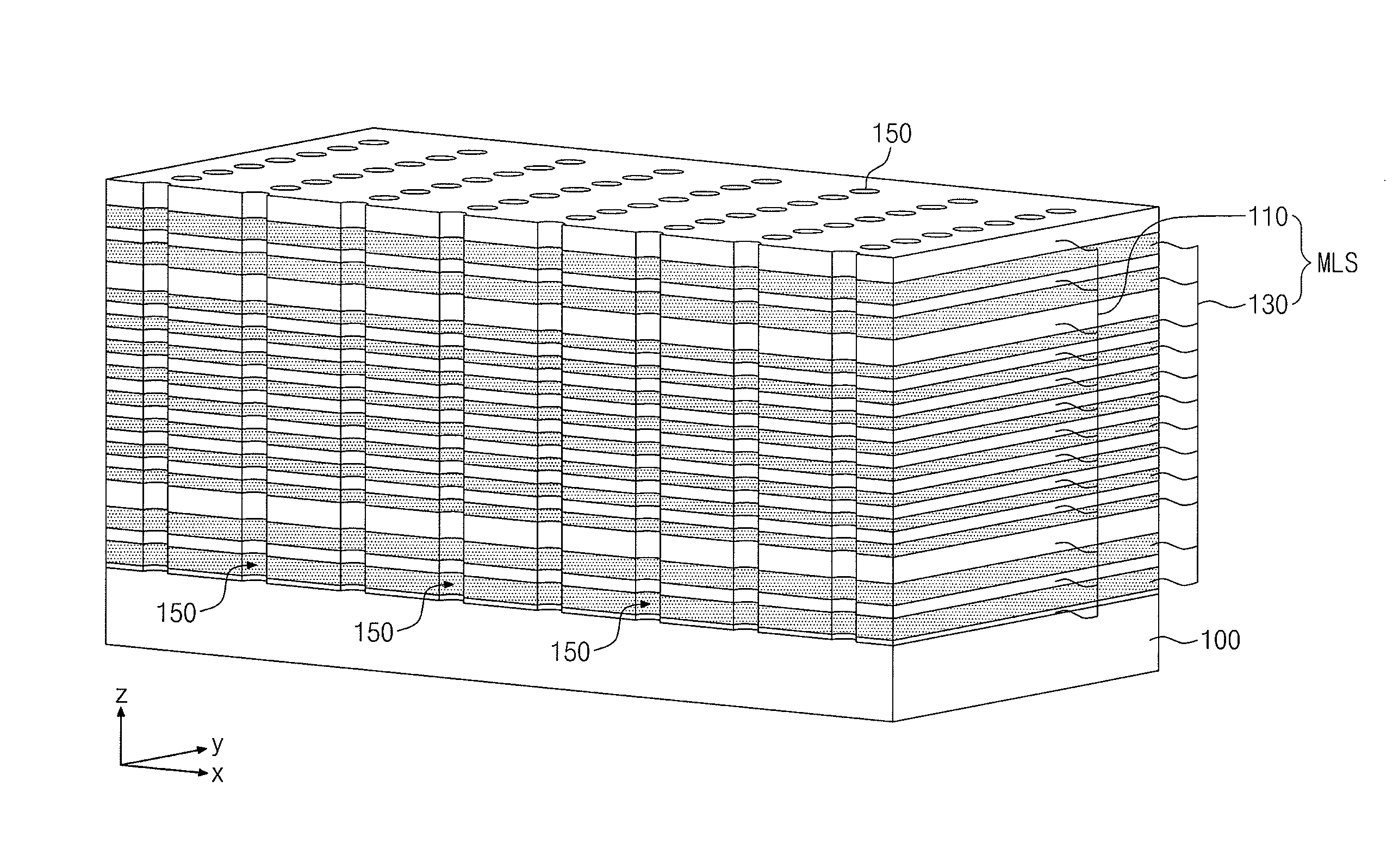
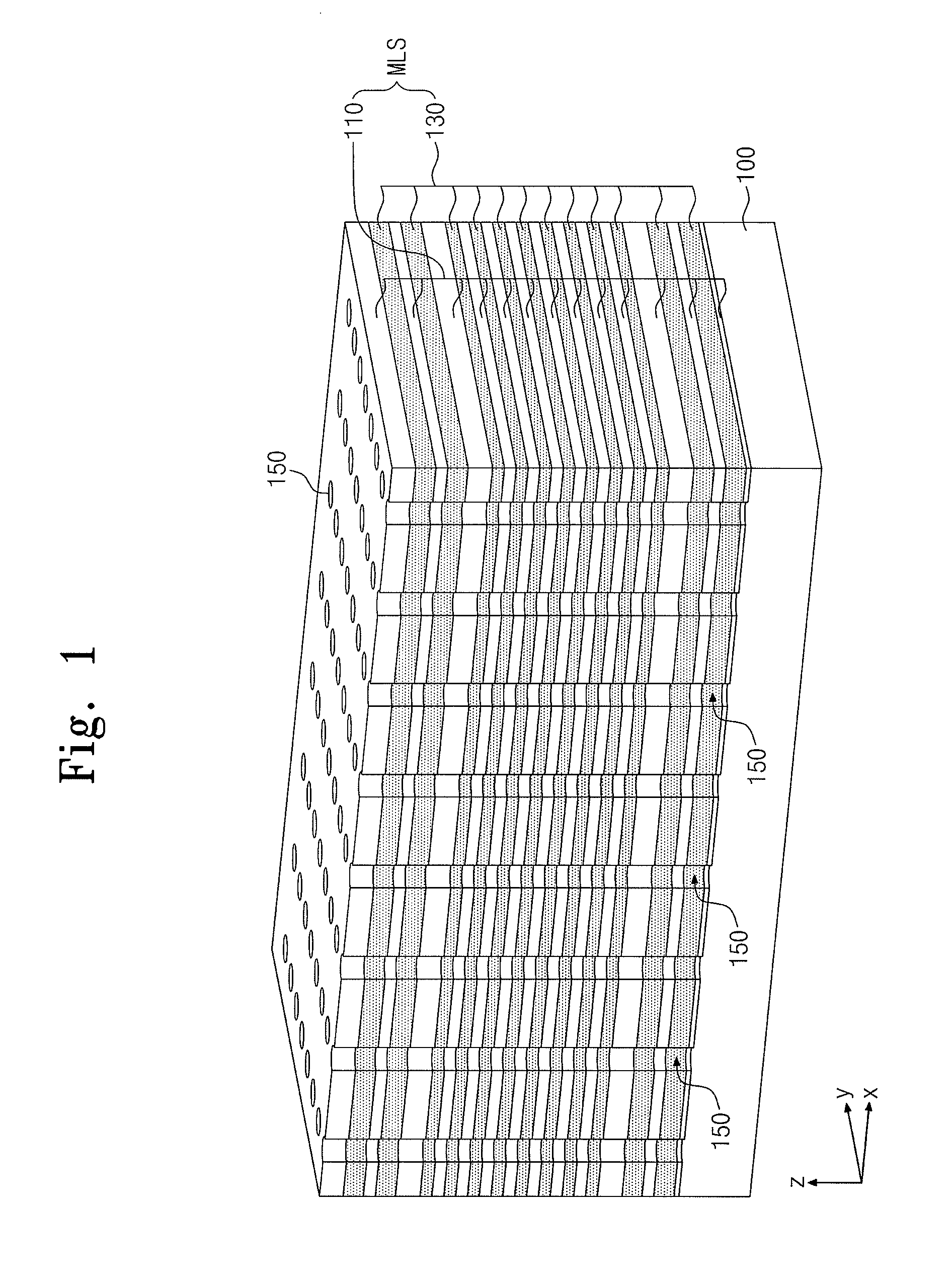
[0039]Referring to FIG. 1, a molding layer structure MLS is formed on a substrate 100, and then is patterned to form active openings 150 for exposing the upper surface of the substrate 100.

[0040]For example, the substrate 100 may be formed of one of semiconductor materials (for example, a silicon wafer), an insulating material (for example, glass), and a semiconductor or conductive member covered with an insulating film. The substrate 100 may have the upper surface parallel to an xy plane. The active openings 150 may be formed two-dimensionally on the substrate 100 or the xy plane.

[0041]The molding layer structure MLS may include ...

second embodiment

[0067]FIGS. 10 through 12, FIG. 13A, FIG. 14A, and FIG. 15A are perspective views illustrating a method of fabricating a three-dimensional semiconductor device according to a second embodiment of the inventive concept. FIG. 13B, FIGS. 14B through 14D, and FIGS. 15B through 15D are perspective views provided to understand the technical spirit of the inventive concept. Specifically, FIGS. 10 through 12 and FIGS. 13A through 15A are perspective views illustrating a method of fabricating the semiconductor device according to the embodiment in a predetermined first view. FIGS. 13B through 15B are perspective views illustrating the semiconductor device illustrated in FIG. 13A, FIG. 14A, and FIG. 15A in a second view different from the first view. FIGS. 14C and 14D are perspective views for explaining the technical features described in FIG. 14A in more detail. FIGS. 15C and 15D are perspective views for explaining the technical features described in FIG. 15A in more detail. For convenienc...

third embodiment

[0093]FIGS. 16A and 16B are a plan view and a perspective view illustrating a three-dimensional semiconductor device according to a third embodiment of the inventive concept, respectively. FIG. 16C is a plan view illustrating a three-dimensional semiconductor device in comparison to the three-dimensional semiconductor device according to the three embodiment of the inventive concept. Since most of the elements were discussed with respect to the previous embodiments, certain details may be omitted for the sake of brevity.

[0094]Referring to FIGS. 16A and 16B, the three-dimensional semiconductor device according to this embodiment of the inventive concept may further include third trenches 203 formed in the connection region CNR. According to an embodiment of the inventive concept, the third trenches 203 may be formed together with the first trenches 201 and the second trenches 202. According to another embodiment of the inventive concept, however, the third trenches may be formed inde...


PUM


Abstract

Provided are a three-dimensional semiconductor device and a method of fabricating the same. The three-dimensional semiconductor device may include a mold structure for providing gap regions and an interconnection structure including a plurality of interconnection patterns disposed in the gap regions. The mold structure may include interlayer molds defining upper surfaces and lower surfaces of the interconnection patterns and sidewall molds defining sidewalls of the interconnection patterns below the interlayer molds.

Description

CROSS-REFERENCE TO RELATED APPLICATIONS[0001]This U.S. non-provisional patent application claims priority under 35 U.S.C. §119 to Korean Patent Application 10-2009-0126854, filed on Dec. 18, 2009, the entire disclosure of which is hereby incorporated by reference herein in its entirety.BACKGROUND[0002]The present disclosure herein relates to a three-dimensional semiconductor device and to a method of fabricating the three-dimensional semiconductor memory device.[0003]Higher integration of semiconductor devices may be required to satisfy consumer demands for superior performance and inexpensive prices. In the case of semiconductor memory devices, since their integration may be an important factor in determining product price, increased integration may especially be required. In the case of typical two-dimensional or planar semiconductor memory devices, since their integration may be mainly determined by the area occupied by a unit memory cell, integration may be significantly influen...

Claims


Application Information

Patent Timeline
Patent Type & Authority Applications(United States)
IPC IPC(8): H01L27/06
CPCH01L27/11551H01L27/11556H01L21/76816H01L27/11582H01L27/11578H01L2924/0002H10B41/20H10B41/27H10B43/20H10B43/27H01L2924/00G03F7/0002G03F7/0037H10B41/10H10B41/30H10B43/10H10B43/30H01L23/291H01L23/3157H01L23/528
Inventor SHIM, JAE-JOOKIM, HANSOOCHO, WONSEOKJANG, JAEHOONCHO, WOOJIN
Owner SAMSUNG ELECTRONICS CO LTD
Why Eureka
Try Eureka