Circuit board and process for fabricating the same

a technology of circuit boards and conductive layers, applied in the field of circuit boards, can solve the problems of poor uniform thickness difficult control of the thickness of the removed portion and easy improper thinning of the conductive layer of the embedded circuit board, etc., to achieve the effect of improving the reliability of the circuit board

Inactive Publication Date: 2011-06-30
UNIMICRON TECH CORP
View PDF5 Cites 14 Cited by
  • Summary
  • Abstract
  • Description
  • Claims
  • Application Information

AI Technical Summary

Benefits of technology

[0008]The invention is directed to a circuit board and a process for fabricating the same in order to improve reliability of the circuit board.

Problems solved by technology

Since the depth of the blind via is different from the depth of the intaglio, the electroplating condition is not easy to be controlled when the electroplating process is performed, which leads to poor uniformity of the thickness of the conductive layer.
Therefore, when a process for removing a portion of the conductive layer at the outside of the intaglio and the blind via is later performed, it is hard to control the thickness of the removed portion of the conductive layer.
Hence, it is easy to improperly thinning the conductive layer of the embedded circuit board or leaving the conductive residue on the dielectric layer.
Moreover, when the build-up wiring structure is fabricated on the aforementioned dielectric layer, the quality of the electroplating process is poor and the yield of the electroplating process is low.
Therefore, the fabrication yield of the build-up wiring structure is decreased and the reliability of the circuit board is decreased as well.

Method used


Image

  • Circuit board and process for fabricating the same
  • Circuit board and process for fabricating the same
  • Circuit board and process for fabricating the same

Examples


Embodiment Construction

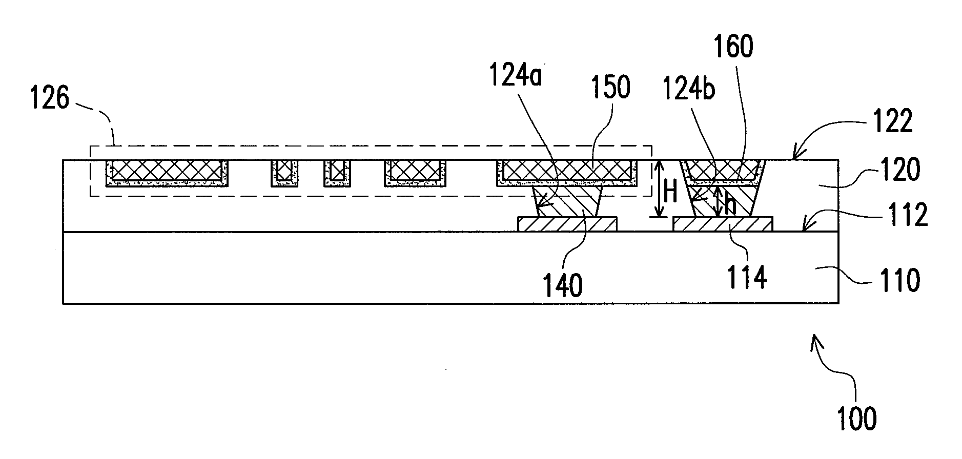
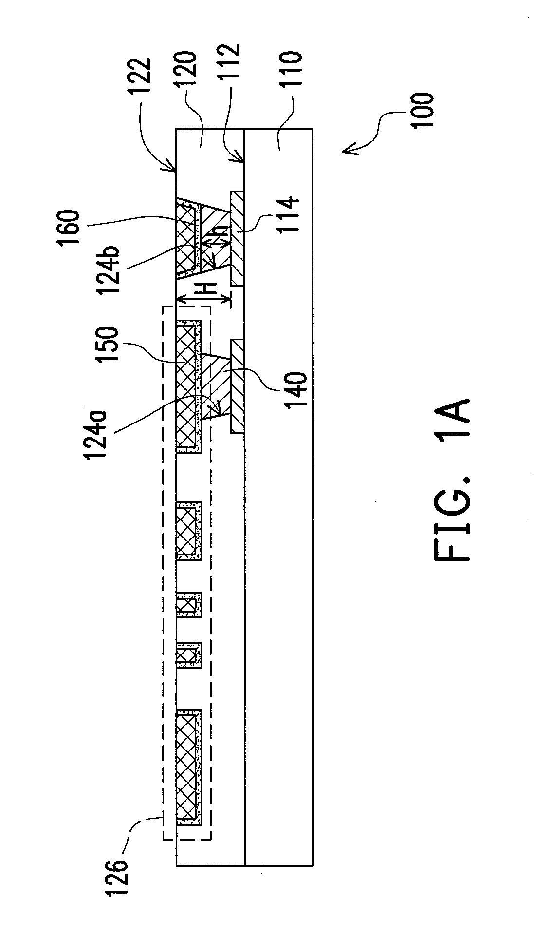
[0042]FIG. 1A is a schematic cross-sectional view illustrating a circuit board according to an embodiment of the invention. As indicated in FIG. 1A, a circuit board 100 includes a circuit substrate 110, a dielectric layer 120, a first conductive layer 140, and a second conductive layer 150. It should be mentioned that the circuit board 100 can have a single circuit layer or multiple circuit layers. That is to say, the circuit board 100 can be a single layer circuit board, a double layer circuit board, or a multi-layer circuit board. In this embodiment, the circuit board 100 depicted in FIG. 1A is a build-up wiring board.

[0043]To be more specific, the circuit substrate 110 has a first surface 112 and a first circuit layer 114. The first circuit layer 114 is disposed on the first surface 112 of the circuit substrate 110. In other words, the first circuit layer 114 is a normal circuit layer (i.e. a non-embedded circuit layer). Note that the first circuit layer 114 is disposed on the fi...


PUM

PropertyMeasurementUnit
thicknessaaaaaaaaaa
conductiveaaaaaaaaaa
heightaaaaaaaaaa

Abstract

A process for fabricating a circuit board is provided. A circuit substrate having a first surface and a first circuit layer is provided. A first dielectric layer having a second surface is formed on the circuit substrate and covers the first surface and the first circuit layer. An antagonistic activation layer is formed on the second surface. The antagonistic activation layer is irradiated by a laser beam to form at least a blind via extended from the antagonistic activation layer to the first circuit layer and an intaglio pattern. A first conductive layer is formed inside the blind via. A second conductive layer is formed in the intaglio pattern and the blind via. The second conductive layer covers the first conductive layer and is electrically connected with the first circuit layer through the first conductive layer. The antagonistic activation layer is removed to expose the second surface.

Description

CROSS-REFERENCE TO RELATED APPLICATION[0001]This application claims the priority benefit of Taiwan application serial no. 98146203, filed on Dec. 31, 2009. The entirety of the above-mentioned patent application is hereby incorporated by reference herein and made a part of this specification.BACKGROUND OF INVENTION[0002]1. Field of Invention[0003]The invention relates to a circuit board and a process for fabricating the same. More particularly, the invention relates to a circuit board having favorable reliability and a process for fabricating the same.[0004]2. Description of Related Art[0005]According to the current technologies, an embedded circuit board has been evolved from a common non-embedded circuit board. In particular, the common non-embedded circuit board is characterized in that circuits therein protrude from a surface of a dielectric layer. By contrast, circuits of the embedded circuit board are buried in the dielectric layer. Currently, a circuit structure of the circuit...

Claims


Application Information

Patent Timeline
Patent Type & Authority Applications(United States)
IPC IPC(8): H05K1/11H05K3/12
CPCH05K3/465H05K2201/0347Y10T29/49165H05K3/06Y10T29/49126H05K1/0298
Inventor TSENG, TZYY-JANGCHIANG, SHU-SHENGCHEN, TSUNG-YUAN
Owner UNIMICRON TECH CORP
Why Eureka
Try Eureka