Semiconductor device and method for producing the same
a semiconductor device and semiconductor technology, applied in the direction of semiconductor/solid-state device manufacturing, semiconductor devices, electrical equipment, etc., can solve the problems of deterioration of the withstand voltage characteristics of this semiconductor device, unstable withstand voltage characteristics, etc., and achieve low on-resistance, good withstand voltage characteristics, and easy production
- Summary
- Abstract
- Description
- Claims
- Application Information
AI Technical Summary
Benefits of technology
Problems solved by technology
Method used
Image

Examples
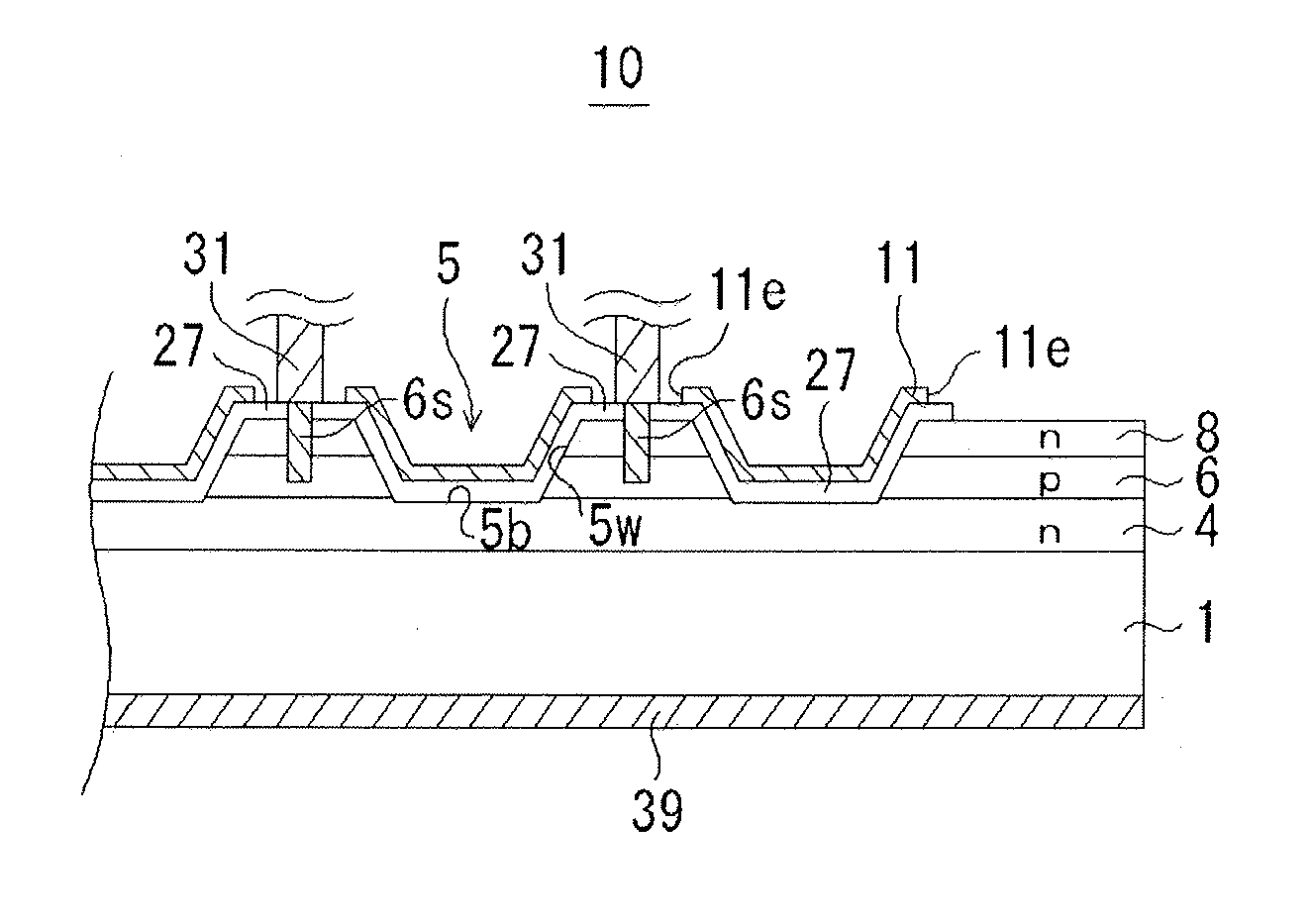
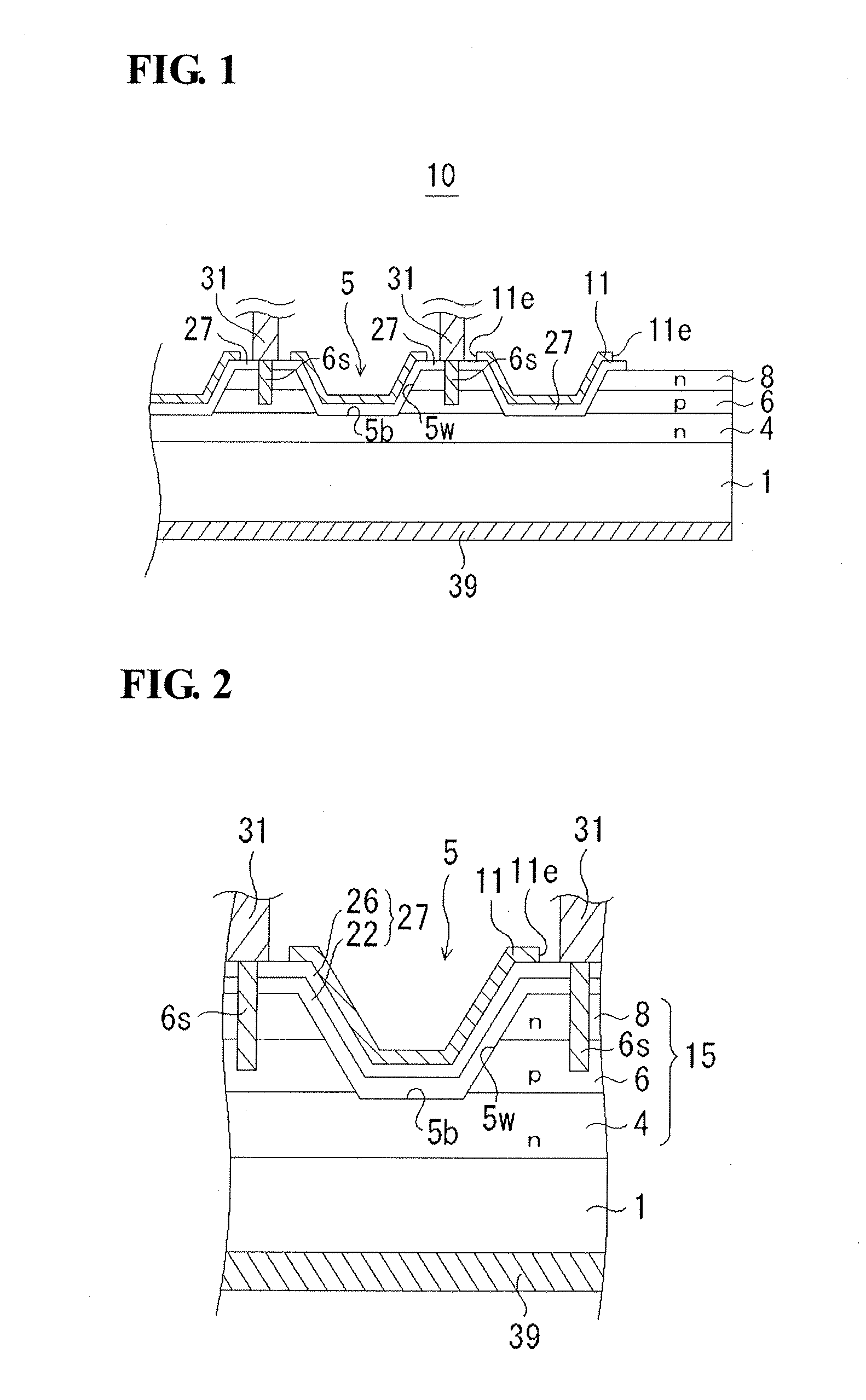
first embodiment
(Modification of First Embodiment)
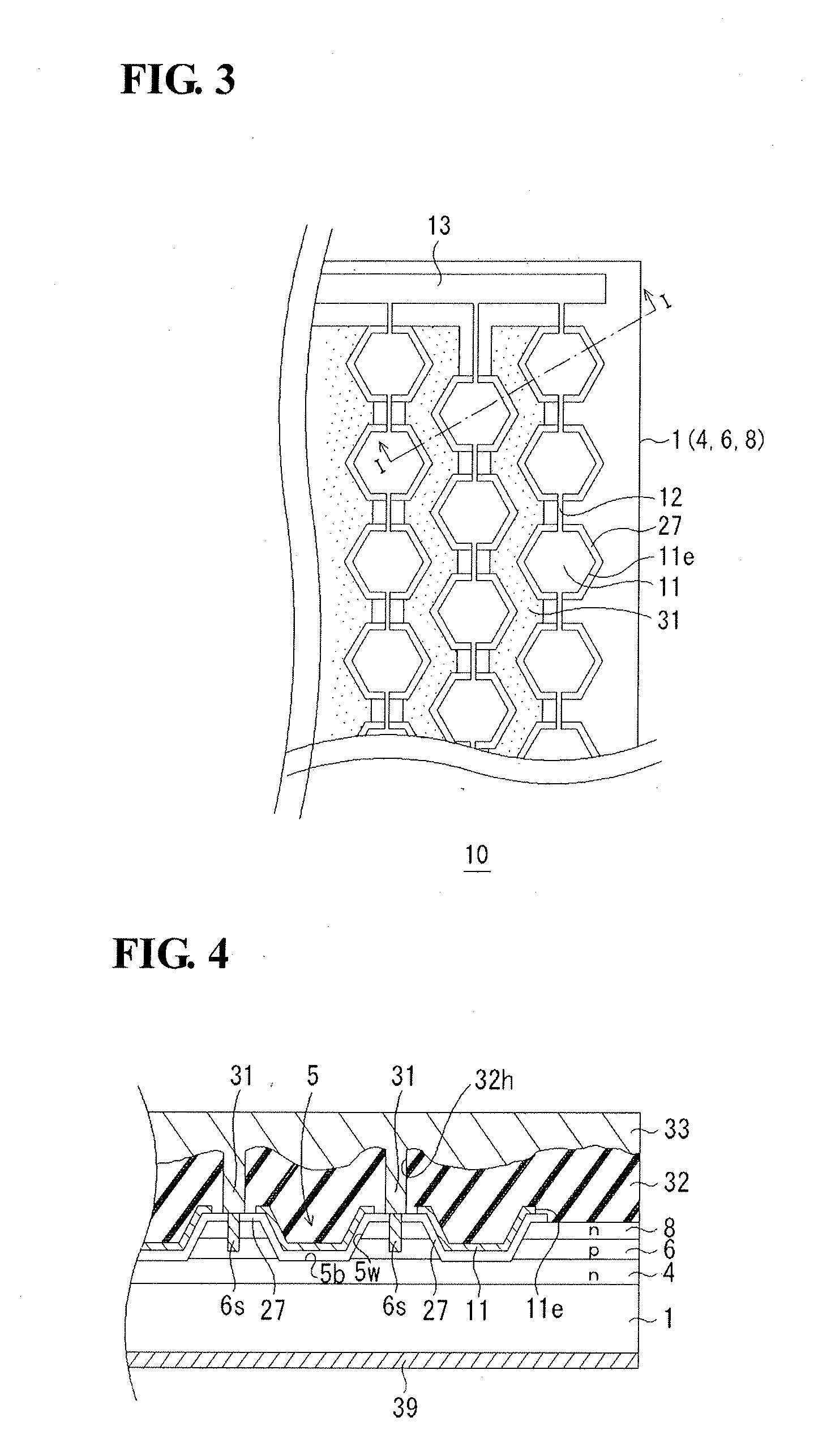
[0086]FIG. 10 is a sectional view showing a vertical GaN-based FET 10 that is a modification of the first embodiment and is also an example of the present invention. A source wiring line and the like are omitted. FIG. 11 is a plan view showing the corner portion of the chip. FIG. 10 is a sectional view taken along line X-X of FIG. 11. The semiconductor device of this modification has a feature of forming a source electrode 31 outside the openings 5 located in the periphery of the chip. In the semiconductor device of the first embodiment shown in FIGS. 1 and 3, a source electrode 31 is not formed outside the openings 5 located in the periphery of the chip. A source electrode is not formed on the right side of the openings 5 located at the right edge of FIG. 1. Therefore, a current does not flow through a channel corresponding to that region, or only a low-density current that comes from a source electrode in other region flows. In contrast, in this m...
second embodiment
[0087]FIG. 12 is a sectional view of a semiconductor device according to a second embodiment of the present invention. The semiconductor device of this embodiment has a feature in which the source electrode 31 and the p-type layer 6 are electrically connected to each other through one conductive portion 6s located in the periphery of the chip. In the semiconductor device of the first embodiment, the substantially ring-shaped hexagonal conductive portion 6s is formed around each of the openings 5 so as to follow the source electrode 31. However, in this embodiment, the source electrode 31 and the p-type layer 6 are electrically connected to each other through one conductive portion 6s that is connected to any one of the source electrode 31 in a single chip. For example, by forming one conductive portion 6s in the periphery of the chip, a simple source-common structure of the p-type layer 6 can be obtained. Thus, a semiconductor device can be produced through simple production steps. ...
third embodiment
[0088]FIG. 13 is a sectional view of a semiconductor device according to a third embodiment of the present invention. The semiconductor device of this embodiment has a feature in which a cap layer 28 is formed between the regrown layer 27 and the gate electrode 11. An i-GaN layer having a lattice constant smaller than that of the AlGaN electron supply layer 26 in the regrown layer 27 is used for the cap layer 28. The cap layer 28 is not limited to the i-GaN layer as long as the cap layer is formed on the AlGaN layer 26 through epitaxial growth and has a lattice constant smaller than that of the AlGaN layer 26. An InGaN layer, an AlGaN layer having a small lattice constant, or an AlInGaN layer can also be used. Furthermore, if an electric field is generated, the cap layer is not necessarily formed on the AlGaN layer 26 through epitaxial growth.
[0089]FIG. 14 shows the case where the cap layer 28 is an i-GaN layer, and the difference in a lattice constant causes spontaneous polarizatio...
PUM
 Abstract
Description
Claims
Application Information