Semiconductor device

a technology of semiconductor devices and semiconductor chips, applied in information storage, static storage, digital storage, etc., can solve the problems of multi-bit error, multi-bit error, soft error between adjacent bits becoming more likely to occur, etc., to achieve the effect of improving reliability in a semiconductor devi

Inactive Publication Date: 2011-06-30
RENESAS ELECTRONICS CORP
View PDF9 Cites 37 Cited by
  • Summary
  • Abstract
  • Description
  • Claims
  • Application Information

AI Technical Summary

Benefits of technology

[0023]That is, it is possible to improve reliability in a semiconductor device having an SRAM.

Problems solved by technology

That is, it has been found that as the SRAM cell becomes finer, a soft error (multi-bit soft error, hereinafter, simply referred to as a multi-bit error) between adjacent bits becomes more likely to occur.
A soft error is a phenomenon in which a number of pairs of electron and hole are generated by the collision of the alpha ray emitted from a package and the neutron beam from the universe to the silicon atoms and when electrons generated particularly in a P well are collected in an N-type diffusion layer, the potential of a storage node is reversed and thereby a malfunction is caused.
In these memory cells, in memory cells neighboring each other in the row direction, the P well is shared on at least one of the right-hand and left-hand sides, and therefore, there is a possibility that the multi-bit error occurs.
However, when an attempt is made to correct a two- or more-bit error, the circuit configuration is complicated and the size of the circuit is increased considerably, which is not desirable.
That is, if a two-bit error occurs at the same time, it is not possible to correct the error by the normal ECC circuit, and therefore, there is a possibility that the multi-bit error occurs at the same time in neighboring cells.

Method used


Image

  • Semiconductor device
  • Semiconductor device
  • Semiconductor device

Examples


first embodiment

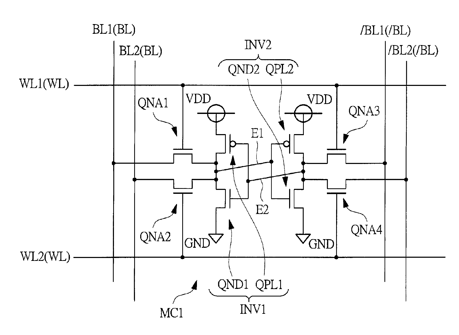
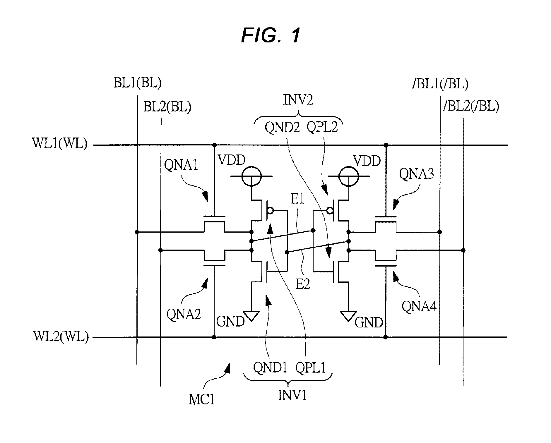
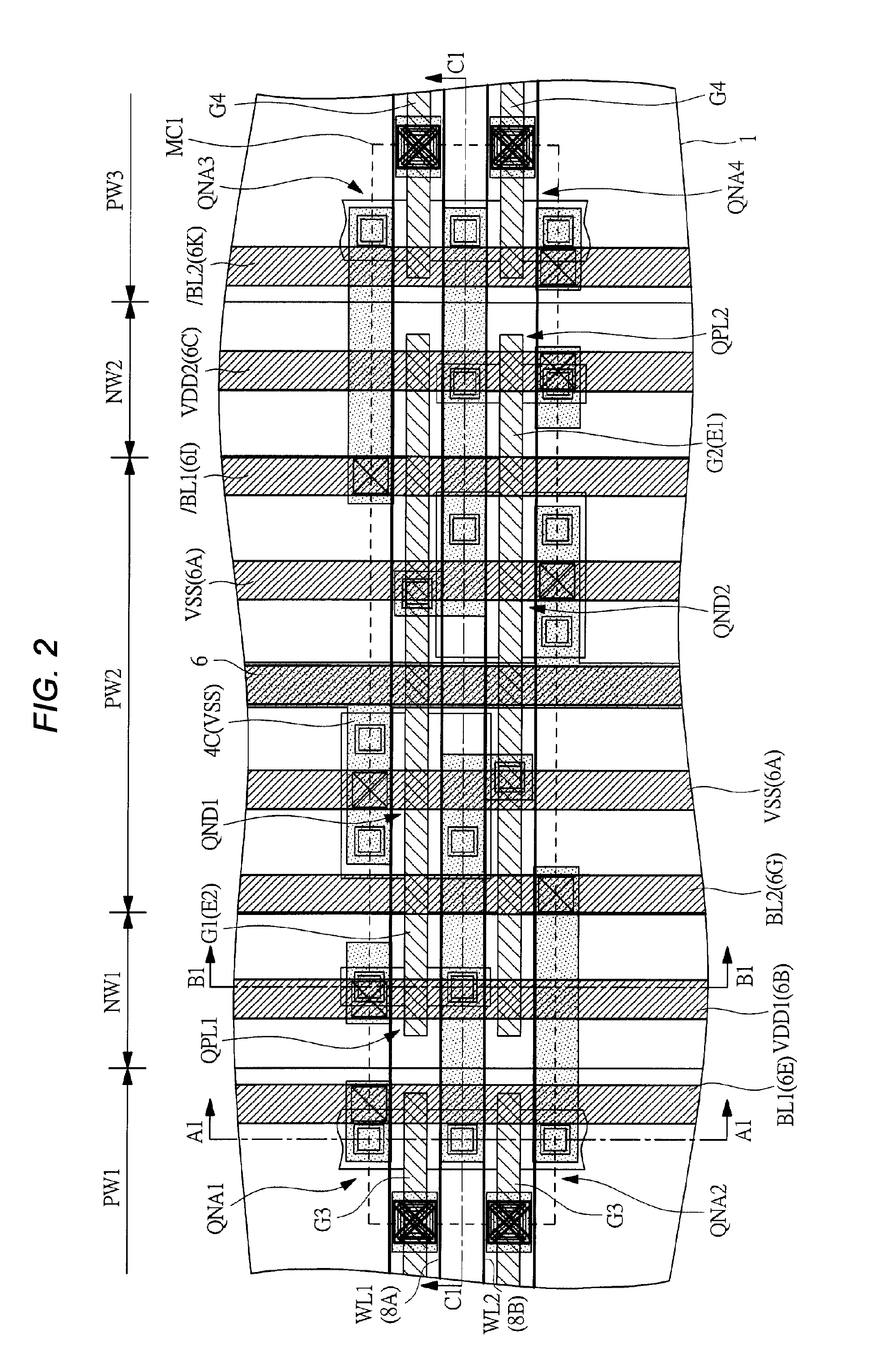
[0071]FIG. 1 shows a circuit diagram of one memory cell (static memory cell) MC1 in a dual-port SRAM in a first embodiment. FIG. 2 shows a plan view of relevant parts of the memory cell MC1 in the first embodiment. FIG. 3 shows a plan view of relevant parts representing from a silicon substrate (semiconductor substrate) 1 to a first wiring layer M1 of the plan view of relevant parts in FIG. 2. FIG. 4 shows a plan view of relevant parts representing from a second wiring layer M2 to a third wiring layer M3 of the plan view of relevant parts in FIG. 2. FIG. 5 shows a section view of relevant parts when viewed in the arrow direction along A1-A1 line, B1-B1 line, and C1-C1 line of the plan view of relevant parts in FIG. 2. FIG. 6 corresponds to the circuit diagram in FIG. 1, particularly, showing an equivalent circuit diagram in which each element and wire are rearranged according to an actual layout. FIG. 7 shows a plan view of relevant parts of three memory cells MCA1, MCA2 and MCA3 ne...

second embodiment

[0119]FIG. 17 shows a plan view of relevant parts of one memory cell (static memory cell) MC2 in a dual-port SRAM in a second embodiment. FIG. 18 shows a plan view of relevant parts representing from the silicon substrate 1 to the first wiring layer M1 of the plan view of relevant parts in FIG. 17. FIG. 19 shows a plan view of relevant parts representing from the second wiring layer M2 to the third wiring layer M3 of the plan view of relevant parts in FIG. 17. FIG. 20 shows an equivalent circuit diagram in which each element and wire are arranged according to an actual layout of the memory cell MC2 in the second embodiment. FIG. 21 shows a plan view of relevant parts of three memory cells MCB1, MCB2 and MCB3 neighboring in the column direction in the dual-port SRAM in the second embodiment. FIG. 22 shows an explanatory diagram of a plurality of memory cells MCB arranged in the row direction and the column direction in the dual-part SRAM in the second embodiment. The dual-port SRAM o...

third embodiment

[0142]In the above-mentioned first and second embodiments, the example is shown, in which the structure of the present invention is applied to the dual-port SRAM. In a third embodiment, an example is shown, in which the structure of the present invention is applied to a single-port SRAM.

[0143]FIG. 27 shows a circuit diagram of one memory cell (static memory cell) MC3 in the single-port SRAM in the third embodiment. FIG. 28 shows a plan view of relevant parts of the memory cell MC3 in the third embodiment. FIG. 29 shows a plan view of relevant parts representing from the silicon substrate 1 to the first wiring layer M1 of the plan view of relevant parts in FIG. 28. FIG. 30 shows a plan view of relevant parts representing from the second wiring layer M2 to the third wiring layer M3 of the plan view of relevant parts in FIG. 28. FIG. 31 corresponds to the circuit diagram in FIG. 27, particularly showing an equivalent circuit diagram in which each element and wire are rearranged accordi...


PUM


Abstract

To improve reliability of a semiconductor device having an SRAM.The semiconductor device has a memory cell including six n-channel type transistors and two p-channel type transistors formed over a silicon substrate. Over the silicon substrate, a first p well, a first n well, a second p well, a second n well, and a third p well are arranged in this order when viewed in a row direction. First and second positive-phase access transistors are disposed in the first p well, first and second driver transistors are disposed in the second p well, and first and second negative-phase access transistors are arranged in the third p well.

Description

CROSS-REFERENCE TO RELATED APPLICATION[0001]The disclosure of Japanese Patent Application No. 2009-292189 filed on Dec. 24, 2009 including the specification, drawings and abstract is incorporated herein by reference in its entirety.BACKGROUND OF THE INVENTION[0002]The present invention relates to technology of a semiconductor device and particularly, to technology effective when applied to a semiconductor device having an SRAM (Static Random Access Memory).[0003]In an electronic device desired to improve performance and increase speed, it is indispensable to mount a microcomputer and in the configuration of a microcomputer, packaging of a high-speed memory with a large capacity is desired. In particular, in order to realize higher-speed processing, it is demanded to increase the capacity of a cache memory. That is, a RAM used by a CPU (Central Processing Unit) of a computer when executing a control program etc. is desired to increase speed and capacity.[0004]As such a RAM, a DRAM (D...

Claims


Application Information

Patent Timeline
Patent Type & Authority Applications(United States)
IPC IPC(8): G11C11/417G11C11/412
CPCG11C11/4125
Inventor NII, KOJI
Owner RENESAS ELECTRONICS CORP
Why Eureka
Try Eureka