Method and device for synthesizing panorama image using scanning charged-particle microscope

a charged particle and microscope technology, applied in the field of methods and devices for generating panorama images, can solve the problems of reducing the operating ratio of the sem apparatus, affecting the quality of the image, and unrealistic manual recipe generation, so as to and reduce the risk of contamination

Active Publication Date: 2011-07-28
HITACHI HIGH-TECH CORP
View PDF8 Cites 38 Cited by
  • Summary
  • Abstract
  • Description
  • Claims
  • Application Information

AI Technical Summary

Benefits of technology

[0028]According to the invention, it is possible to obtain a panorama image synthesis that is robust against contamination and the imaging shift and distortion of an image. Further according to the invention, since the obtained panorama image has wide-field and high resolution, a pattern shape error in the stitching region between the SEPs can be restrained.

Problems solved by technology

The recipe has been manually generated heretofore by an SEM operator, so the labor and time are required.
Further, in order to decide the respective adjustment points and register the registered template in the recipe, it is necessary to actually image the wafer at a low power, resulting in that the generation of a recipe is one of the causes of lowering the operating ratio of the SEM apparatus.
Further, with the development to the microstructure and the complicatedness of a pattern, the number of points requiring evaluation remarkably increases, so that the manual generation of the recipe is becoming unrealistic from a viewpoint of labor and generation time.

Method used


Image

  • Method and device for synthesizing panorama image using scanning charged-particle microscope
  • Method and device for synthesizing panorama image using scanning charged-particle microscope
  • Method and device for synthesizing panorama image using scanning charged-particle microscope

Examples


Embodiment Construction

[0046]This invention provides a method and a device for synthesizing a panorama image using a scanning charged-particle microscope, which may obtain an image (a wide-field image) in a wide imaging region (EP) using a scanning charged-particle microscope (SEM) for observing a fine semiconductor pattern using a panorama image synthesis technique that is robust against contamination and the imaging shift and distortion of an image with high-resolution (high magnification as much as tens of thousands of times to hundreds of thousands of times). The embodiments of the invention will now be described concerning the case of application to the scanning electron microscope (SEM).

[0047]1. SEM

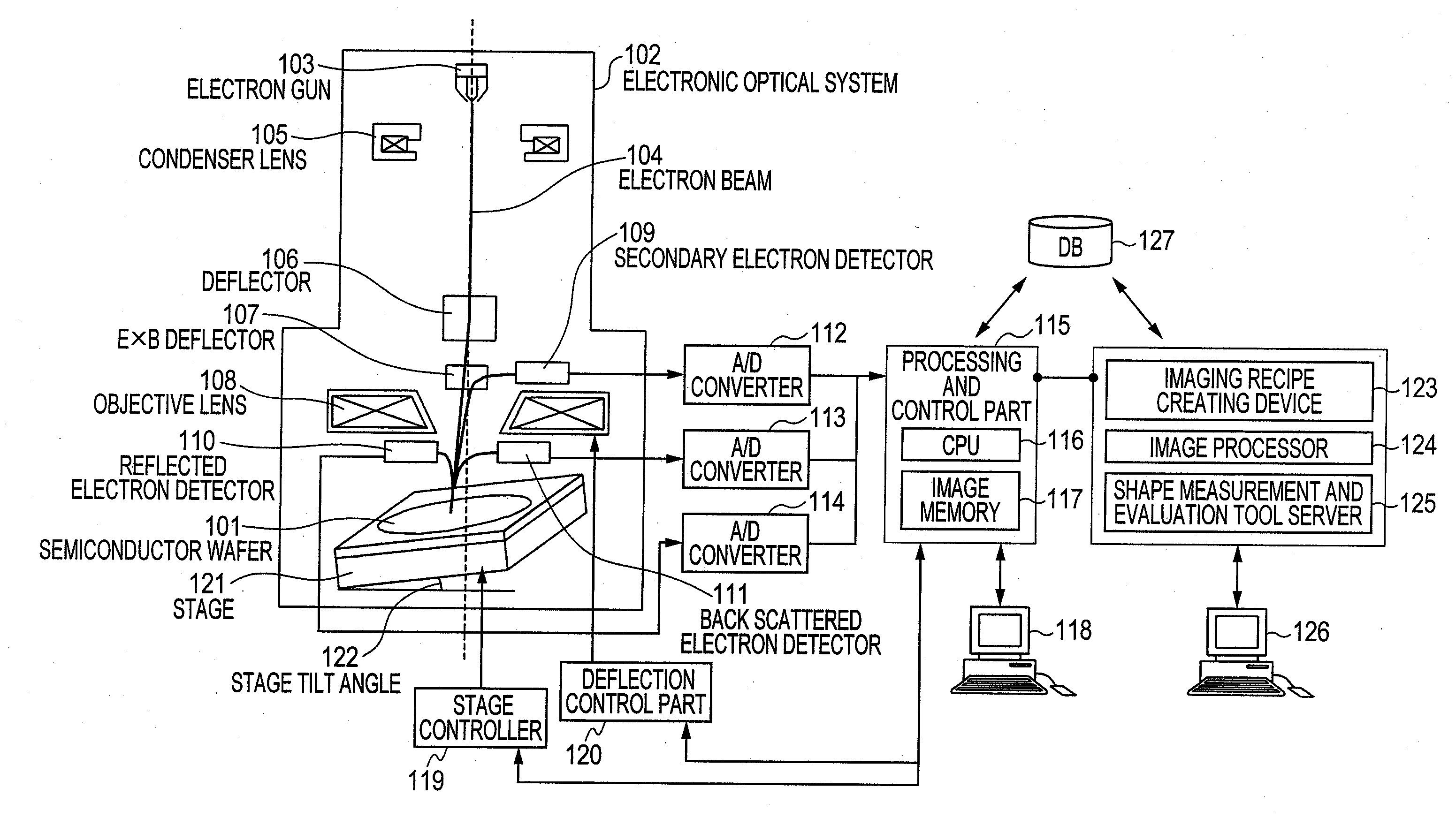
[0048]1.1 SEM Components

[0049]FIG. 1 shows a block diagram of a configuration outline of the SEM for obtaining a secondary electron image (SE image) or a back scattered electron image (BSE image). The SE image and the BSE image are collectively called an SEM image. Further, the image obtained here include...


PUM


Abstract

Provided is a panorama image synthesis technique using a scanning charged-particle microscope and capable of obtaining a panorama image synthesis that is robust against contamination and the imaging shift and distortion of an image in a wide-field imaging region (EP) for semiconductor fine patterns. The panorama image synthesis technique in the wide-field imaging region (EP) using the scanning charged-particle microscope is characterized in that the layout of each adjustment point, each local imaging region, and an imaging sequence comprising the imaging order of the each adjustment point are optimized and created as an imaging recipe.

Description

TECHNICAL FIELD[0001]This invention relates to a method and a device for generating a panorama image that is robust against contamination due to charged-particle irradiation and the imaging shift and distortion of an image by splitting an imaging region into a plurality of local imaging regions, imaging the same, and stitching the picked-up images of the local imaging regions by image processing in order to obtain a wide-field and high-resolution image using a scanning charged-particle microscope.BACKGROUND ART[0002]In forming a wiring pattern on a semiconductor wafer, a method is adopted in which coating material called resist is applied on the semiconductor wafer, an exposure mask (a reticle) of a wiring pattern is superposed on the resist, a visible light ray, ultraviolet rays or an electron beam is applied thereto from above, the resist is photo-sensed (exposed) and developed to thereby form the wiring pattern on the semiconductor wafer, and with this wiring pattern of the resis...

Claims


Application Information

Patent Timeline
Patent Type & Authority Applications(United States)
IPC IPC(8): H04N7/00
CPCG01B15/04H01J37/21H01J37/222H01J37/28H01J2237/2817H01J2237/221H01J2237/24578H01J2237/24592H01J2237/2811H01J2237/21
Inventor MIYAMOTO, ATSUSHIKOTAKI, GOMATSUOKA, RYOICHI
Owner HITACHI HIGH-TECH CORP
Why Eureka
Try Eureka