Semiconductor device, test method thereof, and system

a semiconductor device and test method technology, applied in the direction of resistance/reactance/impedence, testing circuits, instruments, etc., can solve the problems that the i/o compression test cannot be performed concurrently on the respective chips, the operation test needs more time, etc., to achieve the effect of reducing the number of drives and comparators in the tester device, reducing the time required for the i/o compression test, and reducing costs

Active Publication Date: 2011-07-28
LONGITUDE LICENSING LTD
View PDF4 Cites 33 Cited by
  • Summary
  • Abstract
  • Description
  • Claims
  • Application Information

AI Technical Summary

Benefits of technology

[0014]1) An I/O compression test can be performed in parallel concurrently on a plurality of chips including a first chip and a second chip. Therefore, a period of time required for an I/O compression test can be shortened.
[0015]2) For example, when an I/O compression test is performed at th...

Problems solved by technology

As the storage capacity increases, the operation test needs more time.
Therefor...

Method used


Image

  • Semiconductor device, test method thereof, and system
  • Semiconductor device, test method thereof, and system
  • Semiconductor device, test method thereof, and system

Examples


embodiments

[0034]For understanding the present invention, some examples of semiconductor devices 1000 and 3000 to which the present invention is applicable will be described with reference to FIGS. 10, 11, and 12 prior to explanation of embodiments of the present invention. Examples shown in FIGS. 10, 11, and 12 are disclosed in Patent Document 1. As a matter of course, any of those examples is merely for understanding the present invention and never imposes any restriction on the scope of the present invention.

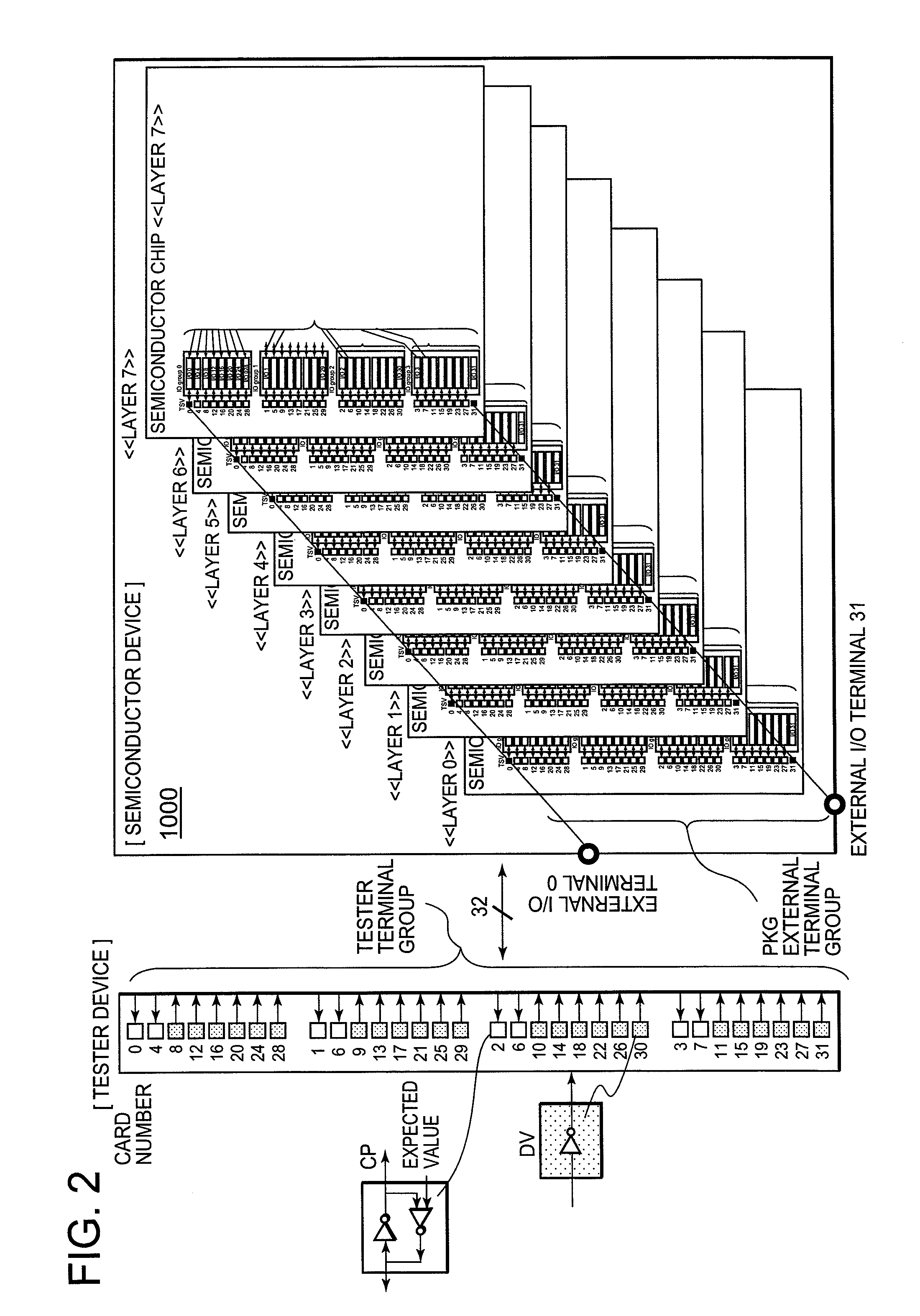
[0035]With reference to FIG. 10, a memory subsystem, i.e., a memory module (semiconductor device) will be summarized as a first example to which the present invention is applicable. A memory module 1000 shown in FIG. 10 includes a module substrate 200, a plurality of dynamic random access memory (DRAM) chips 201, which are two-dimensionally arranged in parallel, a register 202 disposed near a central portion of the module substrate 200, a phase locked loop (PLL) circuit 203, and a seria...


PUM


Abstract

A semiconductor device includes a plurality of chips comprising a plurality of I/O terminals connected in common via through electrodes. Each of the chips includes an I/O compression circuit operable to output a compression result obtained by compression of data of a plurality of internal data buses to a first I/O terminal of the plurality of I/O terminals. Each of the chips also includes a test control circuit having a register group that sets the number of the first I/O terminal. Setting information that assigns different first I/O terminals to different chips is set in the register group. Each of the chips inputs or outputs data with use of the number of the I/O terminal that is different from those in other chips. Thus, the I/O compression circuits can concurrently perform an I/O compression test in parallel in the plurality of chips without a bus fight.

Description

[0001]This application claims the benefit of priority from Japanese patent application No. 2010-16890, filed on Jan. 28, 2010, the disclosure of which is incorporated herein in its entirety by reference.BACKGROUND[0002]1. Field of the Invention[0003]The present invention relates to a semiconductor device, a test method of a semiconductor device, and a system including the semiconductor device.[0004]2. Description of the Related Art[0005]Semiconductor devices having a storage function, e.g., semiconductor memory devices, have been developed so as to increase the degree of integration and the capacity. One of techniques for increasing the degree of integration and the capacity includes stacking a plurality of chips (memory chips) on an I / O chip and connecting the plurality of chips stacked on the I / O chip to each other via through electrodes (TSV: through silicon via), which penetrate the chips in the thickness direction thereof (Patent Document 1: US 2004 / 0257847 A1). Another techniq...

Claims


Application Information

Patent Timeline
IPC IPC(8): G06F19/00
CPCG11C5/04G11C29/40H01L2924/1305H01L2224/16H01L2924/00
Inventor UETAKE, SATOSHIUO, YUJI
Owner LONGITUDE LICENSING LTD
Why Eureka
Try Eureka