Light Emitting Device, Light Emitting Device Package
- Summary
- Abstract
- Description
- Claims
- Application Information
AI Technical Summary
Benefits of technology
Problems solved by technology
Method used
Image

Examples
first embodiment
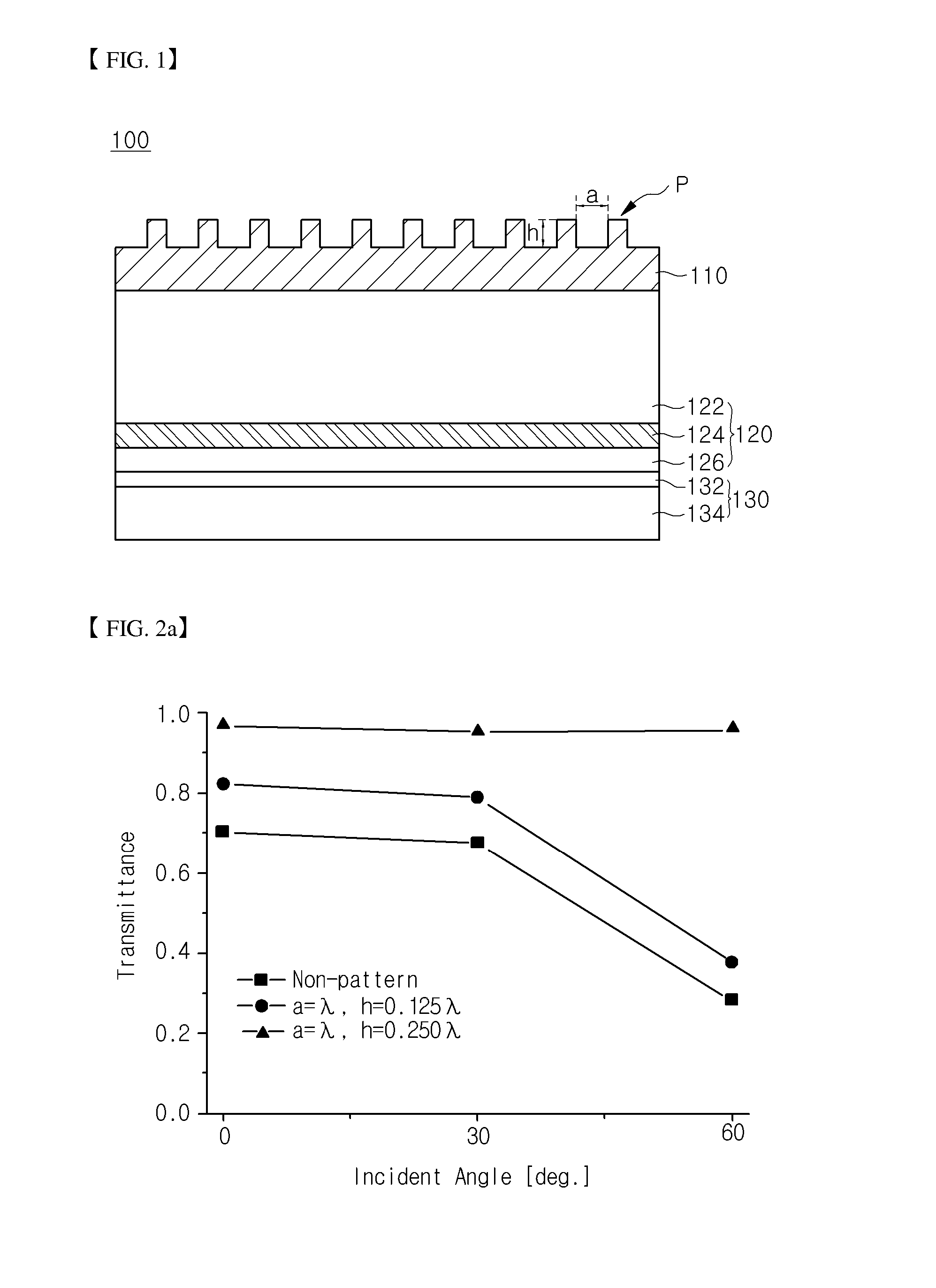
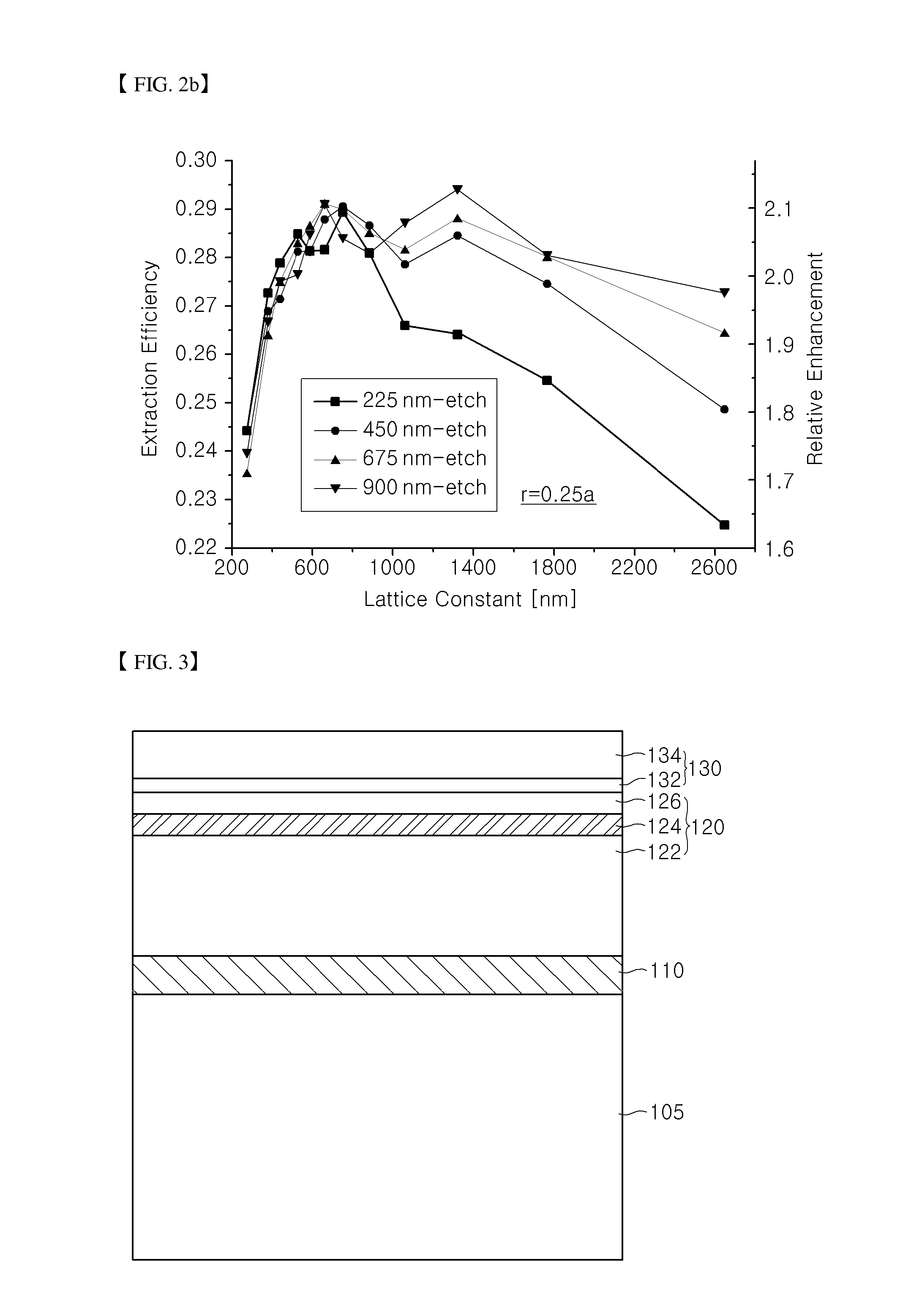
[0028]A light emitting device 100 may include a light emitting structure 120 including a first conductive type semiconductor layer 122, an active layer 124, and a second conductive type semiconductor layer 126 and a light extraction pattern P in which a period (a) exceeds λ / n (where, λ is a wavelength of light emitted from the active layer 124, and n is a refractive index of the light emitting structure 120) on the light emitting structure 120.
[0029]Although the light extraction pattern P is disposed within the light emitting structure 120 in the current embodiment, the present disclosure is not limited thereto. For example, an undoped semiconductor layer 110 may be disposed on the light emitting structure 120, and the light extraction pattern P may be disposed on the undoped semiconductor layer 110. Alternatively, the light extraction pattern P may be disposed on the first conductive type semiconductor layer 122.
[0030]In the current embodiment, the light extraction pattern P may h...
second embodiment
[0082]Also, as shown in FIG. 6, the second embodiment may include a wavelength filter 140 on the light emitting structure 120.
[0083]Also, in the second embodiment, an undoped semiconductor layer 110 may be selectively disposed between the light emitting structure 120 and the wavelength filter 140.
[0084]In case where the second light extraction pattern P2 is disposed on a chip, i.e., in a vertically type LED, the second light extraction pattern P2 may be inserted into an ohmic layer 132 or a reflective layer in a metal pattern or dielectric pattern shape, but is not limited thereto.
[0085]In case where a light extraction pattern is provided on a top end of the chip to improve light extraction efficiency of an LED chip, when light escaping already from a light extraction structure reaches a surface of the top end of the chip again, the light extraction structure may perform a role such as anti-reflection coating to assist the entry of the light into the chip.
[0086]Thus, when the light ...
third embodiment
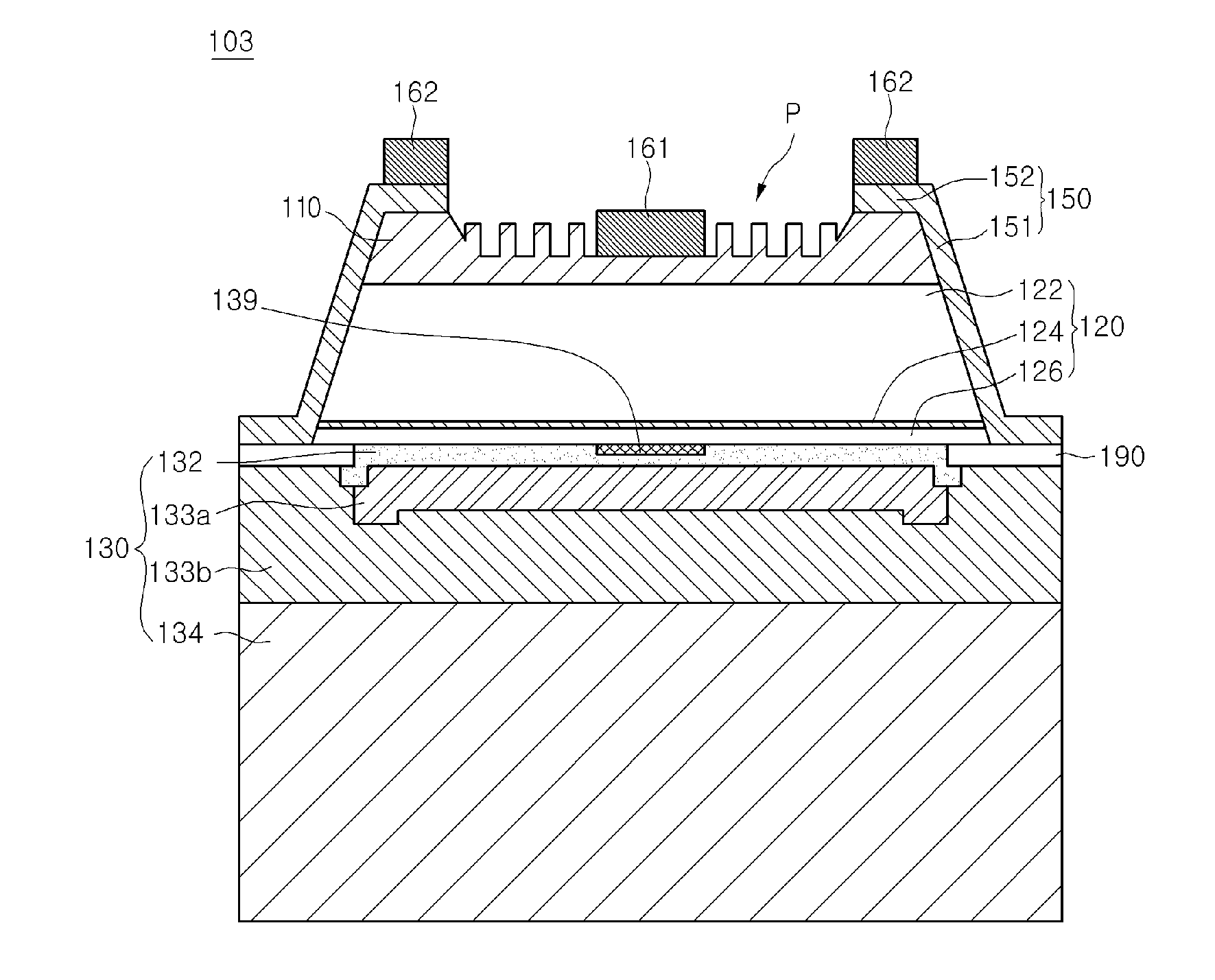
[0096]The light emitting device 103 may include a light emitting structure 120 including a first conductive type semiconductor layer 212, an active layer 214, and a second conductive type semiconductor layer 216, a first dielectric layer 151 on a portion of a top surface of the light emitting structure 120, and a pad electrode 162 on the first dielectric layer 151.
[0097]In the current embodiment, a dielectric layer 150 may include the first dielectric layer 151 and a second dielectric layer 152 on a side surface of the light emitting structure. The first dielectric layer 151 and the second dielectric layer 152 may be connected to each other.
[0098]The current embodiment may include a first electrode 161 on the light emitting structure 120. The pad electrode 162 may be electrically connected to the first electrode 161.
[0099]A light extraction pattern P in which a period (a) exceeds λ / n (where, λ is a wavelength of light emitted from the active layer 214, and n is a refractive index o...
PUM
 Abstract
Description
Claims
Application Information
 - Generate Ideas
- Intellectual Property
- Life Sciences
- Materials
- Tech Scout
- Unparalleled Data Quality
- Higher Quality Content
- 60% Fewer Hallucinations
Browse by: Latest US Patents, China's latest patents, Technical Efficacy Thesaurus, Application Domain, Technology Topic, Popular Technical Reports.
© 2025 PatSnap. All rights reserved.Legal|Privacy policy|Modern Slavery Act Transparency Statement|Sitemap|About US| Contact US: help@patsnap.com