Solid-state imaging device, manufacturing method thereof, electronic apparatus, and semiconductor device

a manufacturing method and semiconductor technology, applied in the direction of semiconductor/solid-state device details, radiation controlled devices, final product manufacturing, etc., can solve the problems of aforementioned problems becoming remarkable, affecting the product yield, and it is difficult to manufacture semiconductor devices such as solid-state imaging devices with high manufacturing efficiency, so as to achieve the effect of improving product yield and high manufacturing efficiency

Active Publication Date: 2011-08-04
SONY SEMICON SOLUTIONS CORP
View PDF4 Cites 27 Cited by
  • Summary
  • Abstract
  • Description
  • Claims
  • Application Information

AI Technical Summary

Benefits of technology

[0020]Embodiments, such as the solid-state imaging device, the method for manufacturing a solid-state imaging device, the electronic apparatus, and the semiconductor device improve product yield and obtain a high manufacturing efficiency.

Problems solved by technology

Therefore, due to the accumulated electric charges, it may be difficult to manufacture the chips as desired, and thus, there may be problems such as degradation of product yield.
For example, properties such as a manufacturing feature, a film formation amount, exfoliation during cleaning vary significantly from a target value, and the aforementioned problems may become remarkable.
In this manner, since the product yield is degraded due to chipping, it may be difficult to manufacture the semiconductor device such as a solid-state imaging device with high manufacturing efficiency.

Method used


Image

  • Solid-state imaging device, manufacturing method thereof, electronic apparatus, and semiconductor device
  • Solid-state imaging device, manufacturing method thereof, electronic apparatus, and semiconductor device
  • Solid-state imaging device, manufacturing method thereof, electronic apparatus, and semiconductor device

Examples


first embodiment

1. First Embodiment

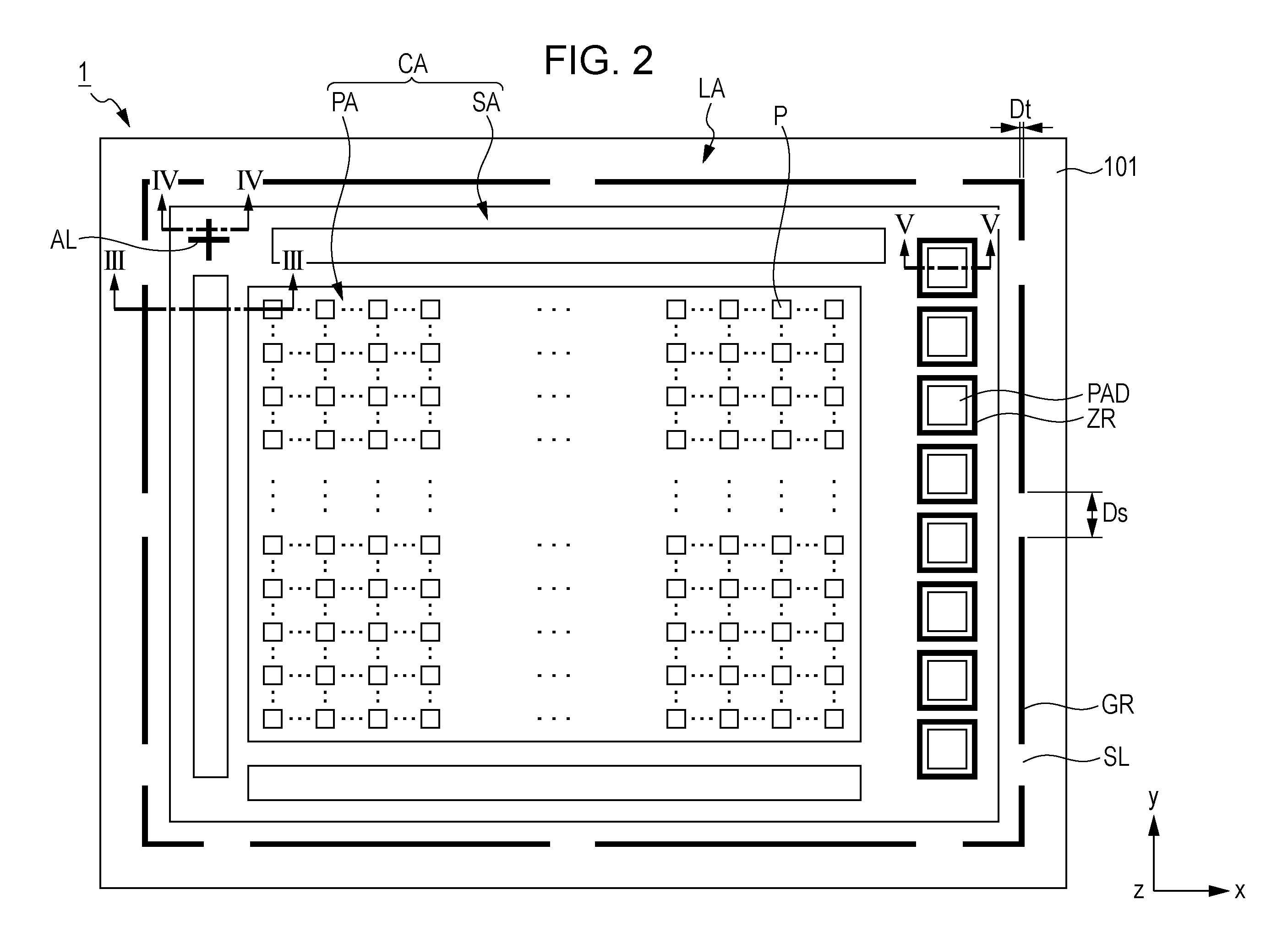
[0046](1) Configuration of Device

[0047](1-1) Configuration of Main Elements of Camera

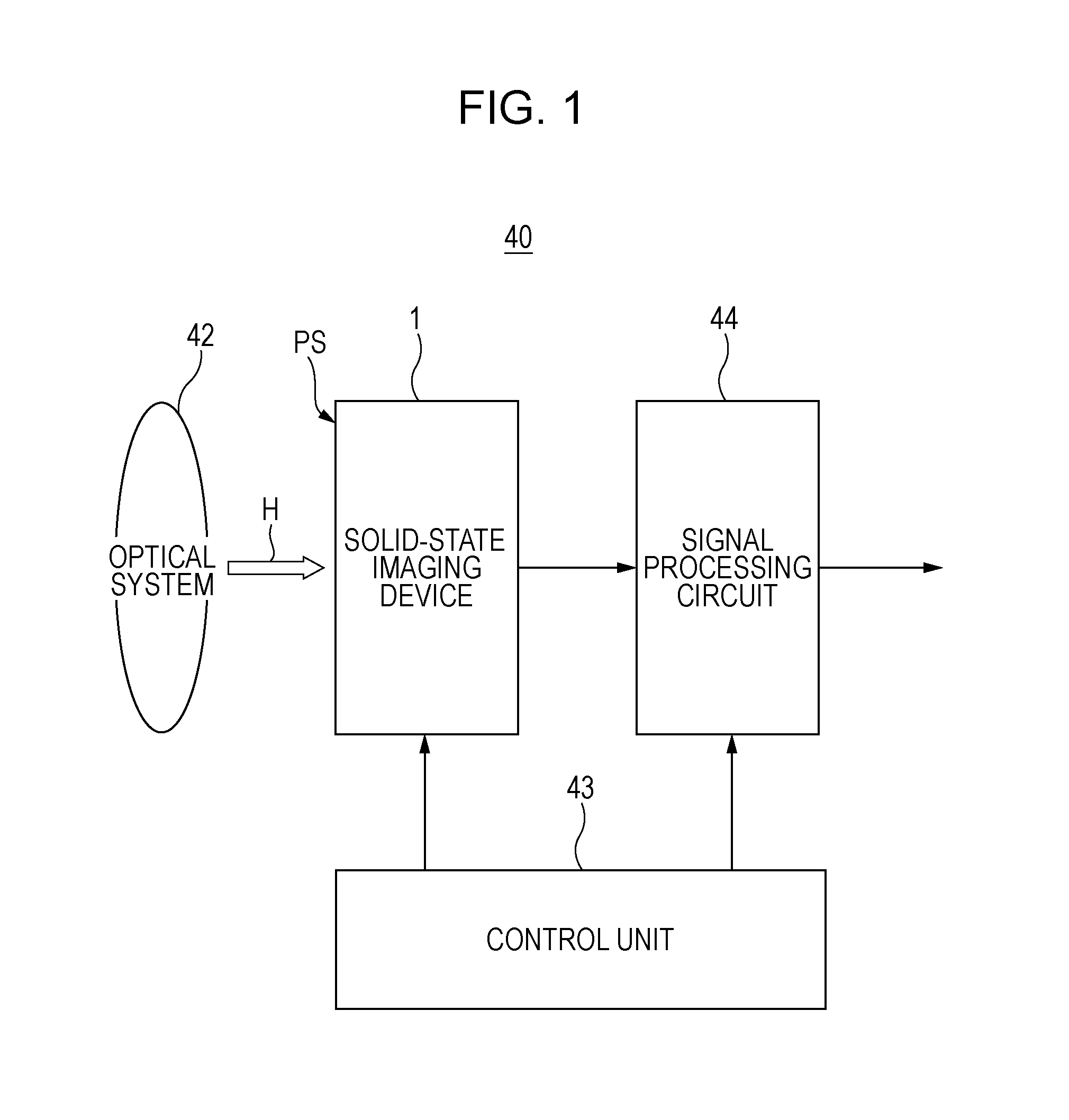
[0048]FIG. 1 is a block diagram illustrating a configuration of the camera 40 according to a first embodiment of the invention.

[0049]Referring to FIG. 1, the camera 40 includes a solid-state imaging device 1, an optical system 42, a control unit 43, and a signal processing circuit 44, each of which will be described in sequence below.

[0050]The solid-state imaging device 1 generates a signal charge by receiving the light (subject image) incident through an optical system 42 from the imaging area PS and photoelectrically converting it. In this case, the solid-state imaging device 1 is driven based on the control signal output from the control unit 43. Specifically, the signal charge is read and output as raw data.

[0051]The optical system 42 includes optical elements such as an imaging lens or diaphragm and is arranged to focus the light H of the subject image on the imaging area PS ...

second embodiment

2. Second Embodiment

[0181](1) Device Configuration

[0182]FIGS. 16 and 17 illustrate main elements of the solid-state imaging device lb according to a second embodiment of the present invention.

[0183]Here, similarly to FIG. 2, FIG. 16 is a top plan view illustrating the overall configuration of the solid-state imaging device lb. Similar to FIG. 3, FIG. 17 illustrates a cross-section taken along the line XVII-XVII of FIG. 16.

[0184]Referring to FIGS. 16 and 17, the present embodiment differs from the first embodiment in that a plurality of guard ring structures are provided. For example, FIGS. 16 and 17 illustrate an embodiment, which includes a first guard ring structure and a second guard ring structure. The first guard ring structure includes guard ring GRa and at least one slit SLa (e.g., at least one portion comprised of the substrate). The second guard ring structure includes guard ring GRb and at least one slit SLb (e.g., at least one portion comprised of the substrate). The pres...

third embodiment

3. Third Embodiment

[0205](1) Device Configuration

[0206]FIGS. 18 and 19 illustrate elements of the solid-state imaging device 1c according to the third embodiment of the present invention.

[0207]Similar to FIG. 2, FIG. 18 is a top plan view illustrating an overall configuration of the solid-state imaging device 1c. Similar to FIG. 3, FIG. 19 illustrates a cross-section taken along the line XIV-XIV of FIG. 18.

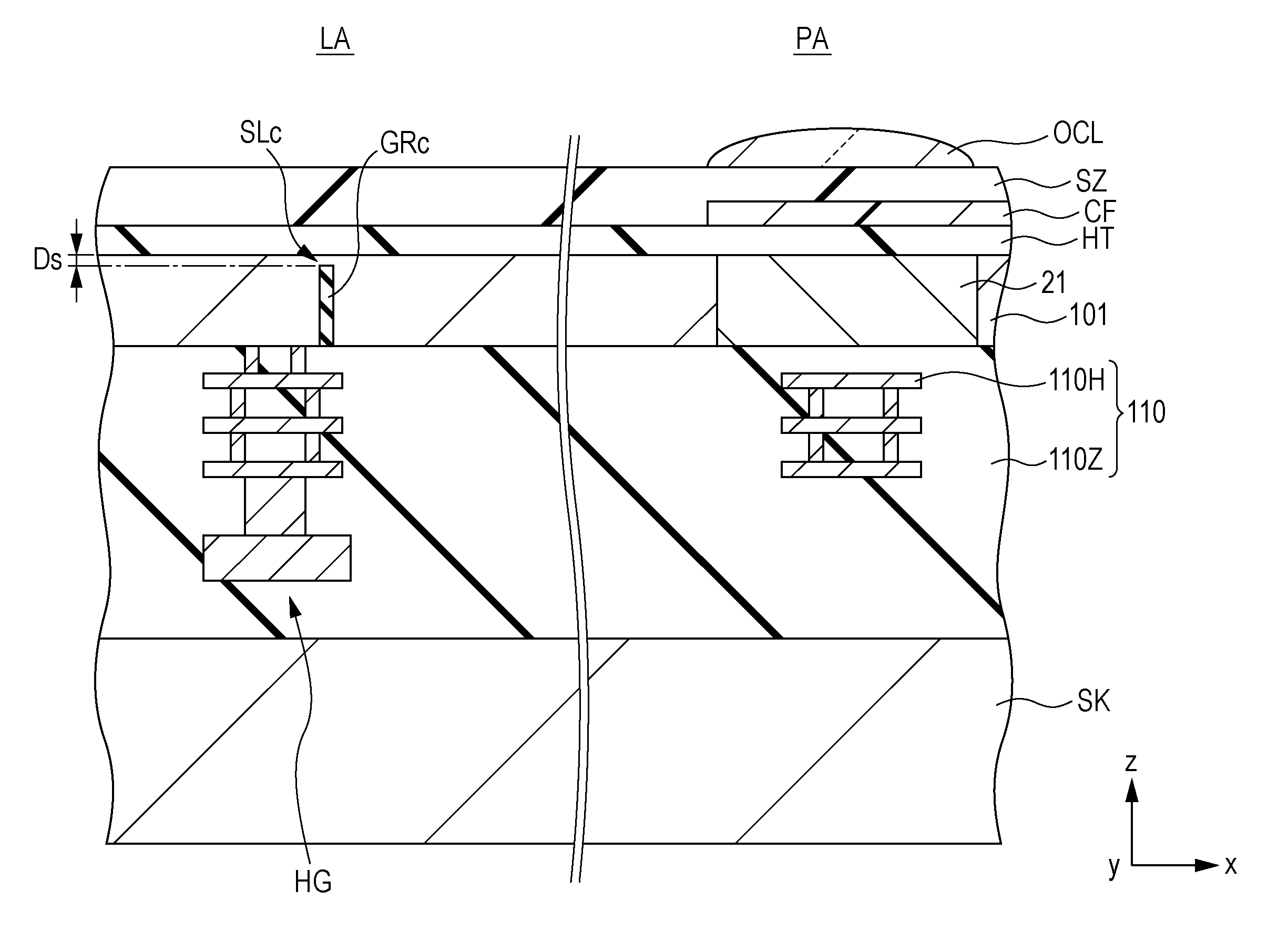
[0208]Referring to FIGS. 18 and 19, the present embodiment differs from the first embodiment in the positions of the slits SLc of the guard ring GRc. The present embodiment is similar to the first embodiment except on this point. Therefore, a description of the repeated elements will be omitted.

[0209]As shown in FIGS. 18 and 19, the guard ring GRc is provided in the scribe area LA.

[0210]The guard ring GRc is provided to surround the circumference of the chip area CA in a rectangular shape in the inner side of the chip area CA side than the end divided through the dicing in the scr...


PUM


Abstract

A semiconductor device includes a substrate, a region including a semiconductor element on the substrate, and at least one guard ring structure provided around the region. The guard ring structure includes a guard ring and at least one portion comprised of the substrate.

Description

RELATED APPLICATION DATA[0001]The present application claims priority to Japanese Priority Patent Application JP 2010-018577 filed in the Japan Patent Office on Jan. 29, 2010, which is incorporated herein by reference in its entirety to the extent permitted by law.BACKGROUND OF THE INVENTION[0002]The present invention relates to a solid-state imaging device, a manufacturing method thereof, an electronic apparatus, and a semiconductor device.[0003]Electronic apparatuses, such as digital video cameras and digital still cameras, include a solid-state imaging device. For example, the solid-state imaging device includes a CMOS (Complementary Metal Oxide Semiconductor) image sensor and a CCD (Charge Coupled Device) image sensor.[0004]In the solid-state imaging device, a plurality of pixels is arranged on the surface of the semiconductor substrate. Each pixel is provided with a photoelectric converter unit. The photoelectric converter unit is, for example, a photodiode which receives the l...

Claims


Application Information

Patent Timeline
Patent Type & Authority Applications(United States)
IPC IPC(8): H01L27/146H01L21/76
CPCH01L21/76H01L31/18H01L27/146H01L27/14636H01L27/14698Y02P70/50
Inventor AKIYAMA, KENTAROTAKIZAWA, MASAAKI
Owner SONY SEMICON SOLUTIONS CORP
Why Eureka
Try Eureka