Method of forming graphene layer

a graphene layer and graphene technology, applied in the direction of vacuum evaporation coating, crystal growth process, polycrystalline material growth, etc., can solve the problems of difficult to ensure the reproducibility of the formation of a graphene layer, difficult to accurately control the number of carbon atoms dispersed in the metal thin film, and chemical vapor deposition (cvd)

Inactive Publication Date: 2011-08-04
KOREA ADVANCED INST OF SCI & TECH
View PDF7 Cites 22 Cited by
  • Summary
  • Abstract
  • Description
  • Claims
  • Application Information

AI Technical Summary

Benefits of technology

[0011]Accordingly, the present invention has been made to solve the above-mentioned problems, and an object of the present invention is to provide a method of forming a graphene layer, by which a uniform graphene layer can be formed on a metal thin film by accurately controlling the amount of carbon ions injected into the metal thin film in order to form the graphene layer on the metal thin film, and by which graphene layers having the same quality can be reproducibly formed on a metal thin film.

Problems solved by technology

However, this method of forming a graphene layer using a chemical vapor deposition (CVD) process is problematic in that it is not easy to accurately control the number of carbon atoms dispersed in the metal thin film during the process of pyrolyzing hydrocarbon gas by heating the metal thin film.
Further, this method of forming a graphene layer using a chemical vapor deposition (CVD) process is problematic in that it is difficult to ensure reproducibility in the formation of a graphene layer because the conditions for forming the graphene layer are sensitive to changes in the kind and amount of impurities remaining in a reactor and generated by performing previous processes.

Method used


Image

  • Method of forming graphene layer
  • Method of forming graphene layer
  • Method of forming graphene layer

Examples


Embodiment Construction

[0027]Hereinafter, preferred embodiments of the present invention will be described in detail with reference to the attached drawings. First, throughout the accompanying drawings, the same reference numerals are used to designate the same or similar components, and redundant descriptions thereof are omitted. Further, in the description of the present invention, when it is determined that the detailed description of the related art would obscure the gist of the present invention, the description thereof will be omitted.

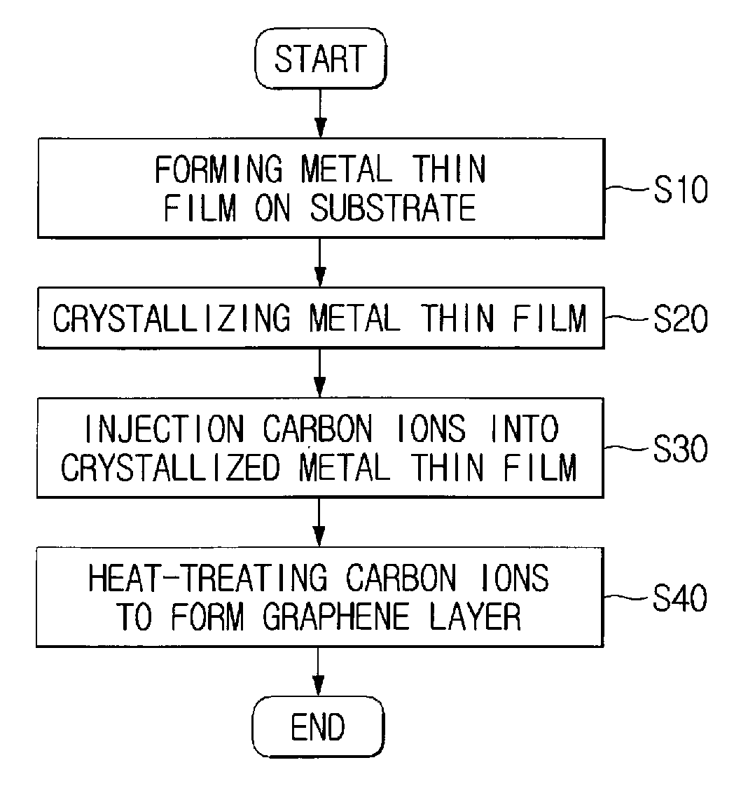
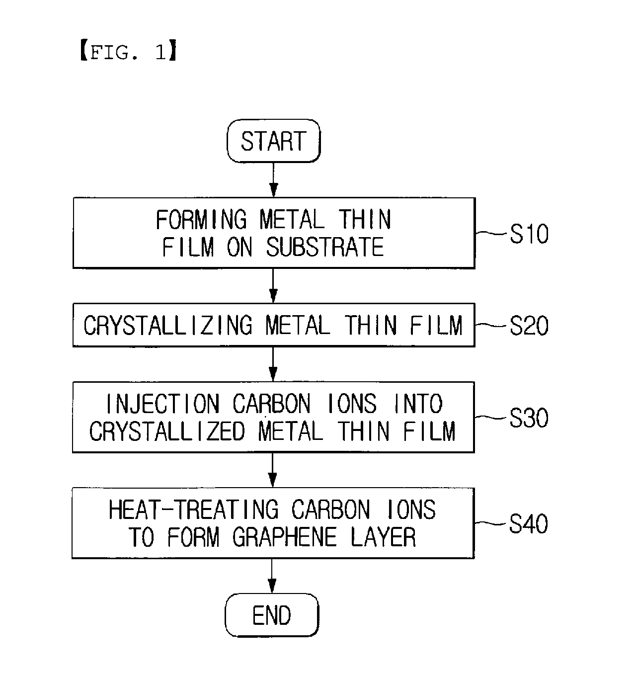
[0028]FIG. 1 is a flowchart showing a method of forming a graphene layer according to an embodiment of the present invention.

[0029]Here, each step of the method of forming a graphene layer according to an embodiment of the present invention may be performed in a reactor.

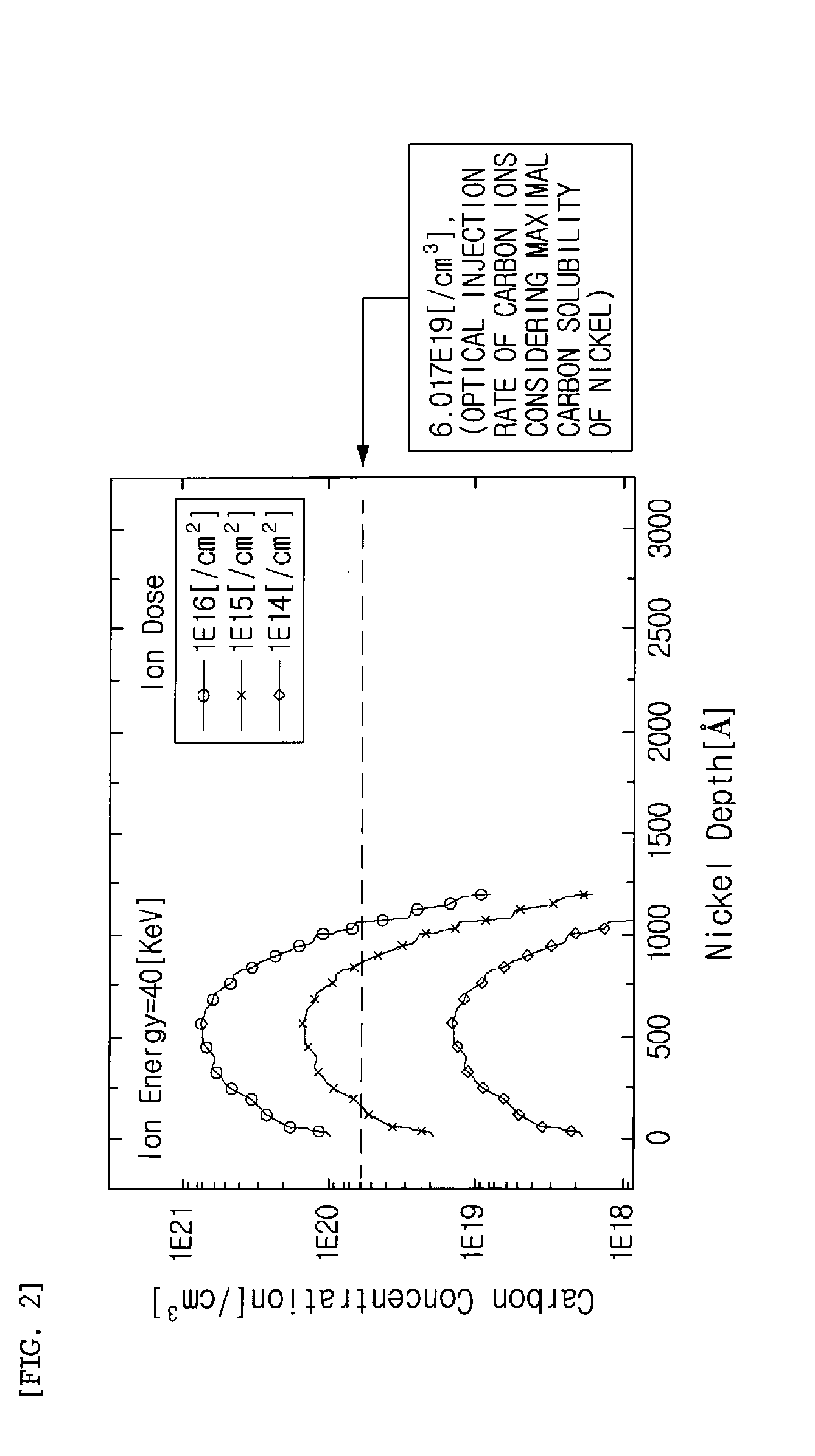
[0030]As shown in FIG. 1, first, in step 10 (S10), a metal thin film is formed on a substrate.

[0031]In this case, the substrate may be a silicon wafer. The metal thin film may be made of any one selecte...


PUM

PropertyMeasurementUnit
temperatureaaaaaaaaaa
electron mobilityaaaaaaaaaa

Abstract

The present invention relates to a method of forming a graphene layer, and, more particularly, to a method of forming a graphene layer which is a two-dimensional thin film composed of carbon atoms arranged in a honeycomb-style lattice and having one atom thick and which is put to practical use in the field of electric devices, transparent electrodes or microwave circuits. The method includes the steps of: (a) forming a metal thin film on a substrate; (b) injecting carbon ions into the metal thin film; and (c) heat-treating the carbon ions injected into the metal thin film to form a graphene layer on the metal thin film. The method is advantageous in that a graphene layer is formed by uniformly injecting an accurate amount of carbon ions into a metal thin film depending on the maximum solubility of carbon in the metal thin film and then heat-treating the injected carbon ions, thus uniformly forming the graphene layer on the metal thin film.

Description

BACKGROUND OF THE INVENTION[0001]1. Technical Field[0002]The present invention relates to a method of forming a graphene layer, and, more particularly, to a method of forming a graphene layer which is a two-dimensional thin film composed of carbon atoms arranged in a honeycomb-style lattice and having one atom thick and which is put to practical use in the field of electric devices, transparent electrodes or microwave circuits.[0003]2. Description of the Related Art[0004]Graphene is a two-dimensional thin film composed of carbon atoms arranged in a honeycomb-style lattice and bound together with a sp2 bond so as to have one atom thick. Graphene has a very high electron mobility of 100,000 cm2 / V·s or more because electrons move in the graphene as if their masses do not exist.[0005]Further, graphene is advantageous in that it can be produced using currently-available CMOS technology because it has a two-dimensional shape unlike carbon nanotubes which have a cylindrical shape. Therefor...

Claims


Application Information

Patent Timeline
Patent Type & Authority Applications(United States)
IPC IPC(8): C23C14/48
CPCC23C14/48B82Y40/00B82Y30/00C30B29/02C01B32/184C23C16/26C01B32/186
Inventor CHO, BYUNG JINMUN, JEONG HUN
Owner KOREA ADVANCED INST OF SCI & TECH
Why Eureka
Try Eureka