
Chemical mechanical polishing apparatus, chemical mechanical polishing method, and control program

Inactive Publication Date: 2011-08-04
TOKYO ELECTRON LTD +1
View PDF4 Cites 5 Cited by
  • Summary
  • Abstract
  • Description
  • Claims
  • Application Information

AI Technical Summary

Benefits of technology

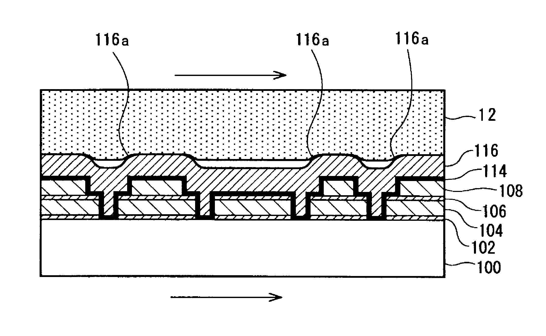
[0014]The present inventor studied a generation mechanism of such a scratch or dishing, and found out that when the semiconductor wafer 100 touches down (touches) the polishing pad 120, a polishing pad 120 scrubs in a direction opposite to the rotating direction of the semiconductor wafer in a part of the surface (surface to be processed) of the semiconductor wafer 100 as shown in FIG. 13, and thus a large shearing stress is applied to the copper 116 of a target object to be polished, specifically protrusions 116a. Accordingly, a small crack is easily generated on the surface of the copper 116 and slurry enters into the small crack, and thus the corresponding spot is excessively polished, thereby causing a scratch or dishing. It is thought that since the copper of the target object to be polished is a relatively soft metal and the low-k organic film forming the interlayer insulating film is weak against an external stress and thus easily gathers a shearing stress, the crack is generated during touch down.
[0033]According to a chemical mechanical polishing apparatus, a chemical mechanical polishing method, or a control program of the present invention, generation of a scratch or dishing is prevented via the above configuration and effects when copper deposited on an interlayer insulating film formed of an organic low-k film is polished during a damascene process, thereby forming an embedded copper wire having excellent precision of is planarization and stability of electric characteristics.

Problems solved by technology

In a conventional wire forming process with respect to the multi-layer wire structure, a metal wire pattern is formed by processing a metal film of Al or the like deposited on an insulating film via lithography and dry etching, but the Al wire has low electro-migration resistance, relatively high electric resistance, and wire delay.

Method used


Image

  • Chemical mechanical polishing apparatus, chemical mechanical polishing method, and control program
  • Chemical mechanical polishing apparatus, chemical mechanical polishing method, and control program
  • Chemical mechanical polishing apparatus, chemical mechanical polishing method, and control program

Examples


Embodiment Construction

[0064]Hereinafter, very suitable embodiments of the present invention will be described with reference to FIGS. 1 through 9.

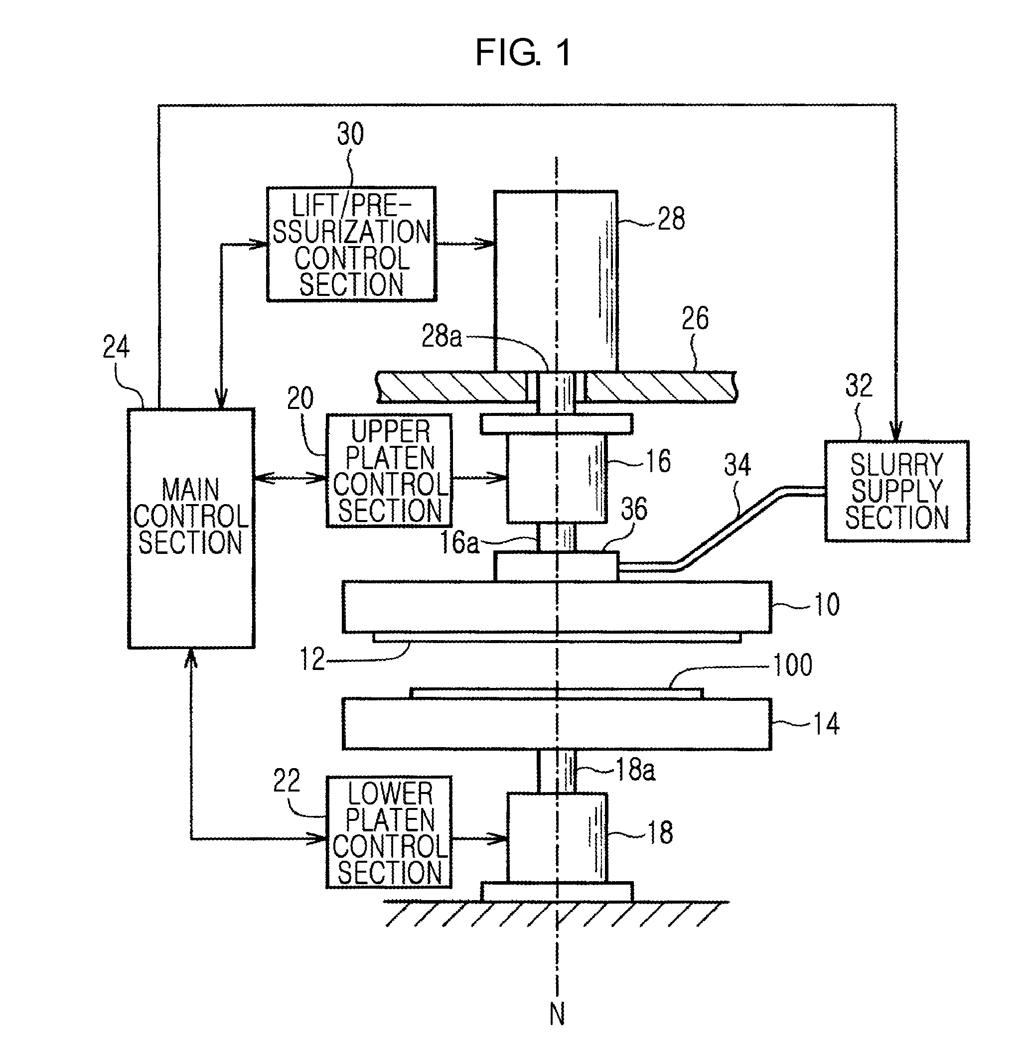
[0065]FIG. 1 is a diagram showing main elements of a CMP (chemical mechanical polishing) apparatus according to an embodiment of the present invention. The CMP apparatus may be used very suitably in a damascene process for forming an embedded copper wire, and for example, may be used in the CMP process ((d) to (e) of FIG. 10) for is planarly polishing the copper 116 deposited on the low-k organic film (interlayer insulating film) 108 of the semiconductor wafer 100 in the damascene process of FIG. 10.

[0066]In the CMP apparatus, a polishing pad 12 is attached to a rotating head (upper platen) 10 that is spin-rotatable and liftable, and a semiconductor wafer 100 is disposed face-up on a rotating table (lower platen) 14 that is spin-rotatable and stationary. The rotating table 14 includes a holding means, for example, a vacuum chuck (not shown), for holding the sem...


PUM

PropertyMeasurementUnit
Angular velocityaaaaaaaaaa

Abstract

Scratches and dishing are prevented from being generated when copper, which is deposited on an interlayer insulating film formed of an organic low-k film, is polished during a damascene process. In the CMP apparatus, while a rotating center axis of a rotating head, which has a polishing pad attached thereon, and a rotating center axis of a rotating table, which has a semiconductor wafer disposed face-up thereon, are aligned on the same vertical line, and the rotating head and the rotating table are spin-rotating in the same direction, the rotating head is lowered and the polishing pad touches the semiconductor wafer on the rotating table. Accordingly the polishing pad is prevented from scrubbing in a direction opposite to the rotating direction of the semiconductor wafer in the entire surface of the semiconductor wafer.

Description

TECHNICAL FIELD[0001]The present invention relates to a chemical mechanical polishing apparatus, chemical mechanical polishing method, and a control program, which are used in a damascene process for forming a copper wire by embedding copper in an interlayer insulating film formed of an organic low-k film.BACKGROUND ART[0002]A recent semiconductor integrated circuit, specifically an LSI (Large Scale Integrated Circuit) has a multi-layer wire structure, in which a plurality of wire layers overlap is each other, for minuteness and high integration. In a conventional wire forming process with respect to the multi-layer wire structure, a metal wire pattern is formed by processing a metal film of Al or the like deposited on an insulating film via lithography and dry etching, but the Al wire has low electro-migration resistance, relatively high electric resistance, and wire delay. In this regard, recently, a damascene process of a copper wire is employed in the multi-layer wire forming pr...

Claims


Application Information

Patent Timeline
IPC IPC(8): H01L21/306C23F1/08B24B37/10H01L21/304
CPCH01L21/3212B24B37/04H01L21/28H01L21/304
Inventor MATSUOKA, TAKAAKIOHMI
Owner TOKYO ELECTRON LTD
Learn More