Method of manufacturing semiconductor device, and semiconductor device

a manufacturing method and technology of semiconductor devices, applied in the direction of semiconductor devices, electrical appliances, transistors, etc., to achieve the effect of reducing the implantation mask

Active Publication Date: 2011-08-11
RENESAS ELECTRONICS CORP
View PDF12 Cites 15 Cited by
  • Summary
  • Abstract
  • Description
  • Claims
  • Application Information

AI Technical Summary

Benefits of technology

[0015]In accordance with the method of manufacturing the semiconductor device according to the present invention, it is possible to reduce implantation masks for forming the halo regions of the transistor of the first conductivity type and the transistor of the second conductivity type.

Problems solved by technology

However, in the SRAM including the access transistors described above has the following problem.

Method used


Image

  • Method of manufacturing semiconductor device, and semiconductor device
  • Method of manufacturing semiconductor device, and semiconductor device
  • Method of manufacturing semiconductor device, and semiconductor device

Examples


embodiment 1

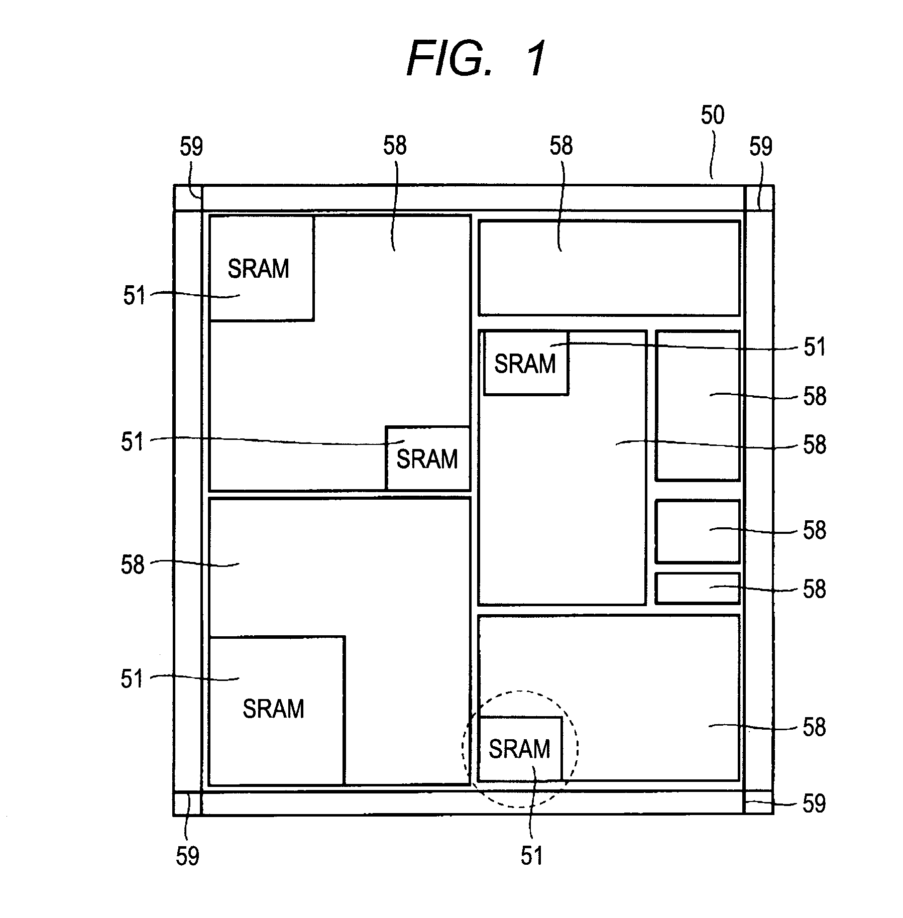
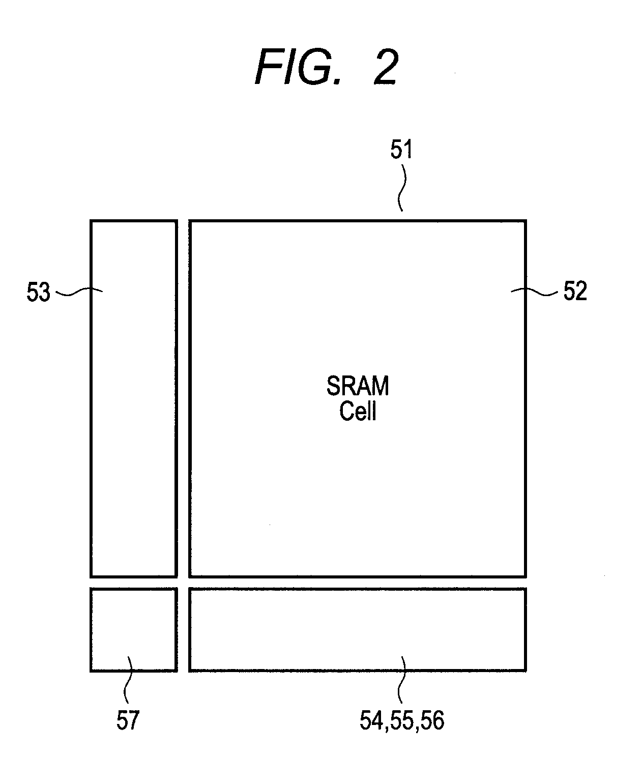
[0133]First, a description will be given of an example of a semiconductor device referred to as a SOC in which a SRAM is applied to a memory cell. As shown in FIG. 1, in a semiconductor device 50, a plurality of logic circuits 58 which implement the respective specific functions of a micro-control unit, an analog-digital converter, a digital-analog converter, a bus controller, and the like, SRAMs 51 coupled to some of the logic circuits to temporarily store data therein, and the like are mounted on one chip. IO regions 59 are formed so as to surround the logic circuits 58 and the SRAMs 51. As shown in FIG. 2, each of the SRAMs 51 includes a SRAM memory cell array 52 having a plurality of memory cells arranged in a matrix, an X-decoder 53, a Y-decoder 54, a sense amplifier 55, a line driver 56, and a main control circuit 57.

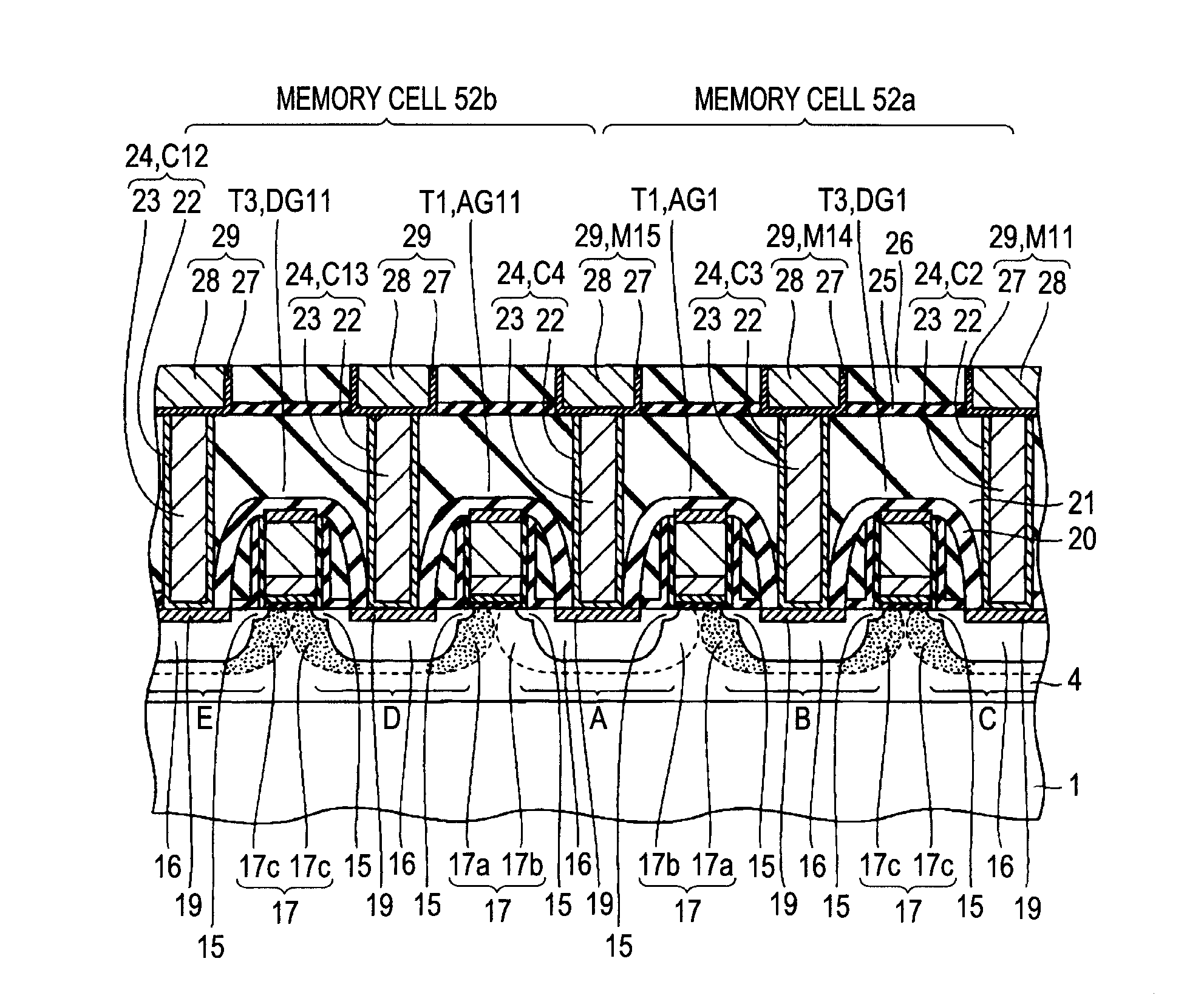
[0134]Next, a description will be given of an equivalent circuit of the SRAM memory cell. As shown in FIG. 3, the SRAM memory cell includes a flip-flop in which t...

embodiment 2

[0201]In the embodiment described above, the exemplary case has been described in which the impurities of the pair of halo regions of each of the drive transistors are the same. Here, a description will be given of a semiconductor device in which the impurity concentrations of the pair of halo regions of each of the access transistors are set asymmetrically, and the impurity concentrations of the pair of halo regions of each of the drive transistors are also set asymmetrically.

[0202]First, a description will be given of an equivalent circuit of a SRAM memory cell. As shown in FIG. 41, in the access transistors T1 and T2 of each of the memory cells in the semiconductor device according to Embodiment 2, the respective pairs of halo regions 17 formed therein include the halo regions 17a coupled to the storage nodes SN1 and SN2 and the halo regions 17b coupled to the bit lines BL and / BL, and the impurity concentrations of the halo regions 17a are set higher than the impurity concentrat...

embodiment 3

[0229]Here, a description will be given of the case where, as an impurity implanted to form the halo regions of the nMIS transistors, carbon (C) is implanted in addition to the p-type impurity.


PUM


Abstract

There are provided a method of manufacturing a semiconductor device which achieves a reduction in implantation masks, and such a semiconductor device. By implanting boron into NMOS regions using a resist mask and another resist mask as the implantation masks, p-type impurity regions serving as the halo regions of access transistors and drive transistors are formed. By further implanting phosphorus or arsenic into a PMOS region using another resist mask as the implantation mask, n-type impurity regions serving as the halo regions of load transistors are formed.

Description

CROSS-REFERENCE TO RELATED APPLICATIONS[0001]The disclosure of Japanese Patent Application No. 2010-24513 filed on Feb. 5, 2010 including the specification, drawings and abstract is incorporated herein by reference in its entirety.BACKGROUND OF THE INVENTION[0002]The present invention relates to a method of manufacturing a semiconductor device and the semiconductor device, and particularly to a method of manufacturing a semiconductor device including a SRAM and such a semiconductor device.[0003]As a form of a semiconductor device, there is a semiconductor device called a SOC (System On Chip). In a semiconductor device of this type, a plurality of logic circuits, memory cells, and the like are mounted on one chip. A description will be given herein of a semiconductor device in which a SRAM (Static Random Access Memory) is applied to a memory cell of such a semiconductor device.[0004]A SRAM memory cell includes a flip-flop in which two inverters are cross-coupled, and two access trans...

Claims


Application Information

Patent Timeline
Patent Type & Authority Applications(United States)
IPC IPC(8): H01L27/088H01L21/8234
CPCH01L21/823412H01L27/1104H01L27/11H10B10/00H10B10/12
Inventor NII, KOJIIGARASHI, MOTOSHIGE
Owner RENESAS ELECTRONICS CORP
Why Eureka
Try Eureka