

Semiconductor module, method for fabricating the semiconductor module, and mobile apparatus
- Summary
- Abstract
- Description
- Claims
- Application Information
AI Technical Summary
Benefits of technology
Problems solved by technology
Method used
Image

Examples
first embodiment
(First embodiment)
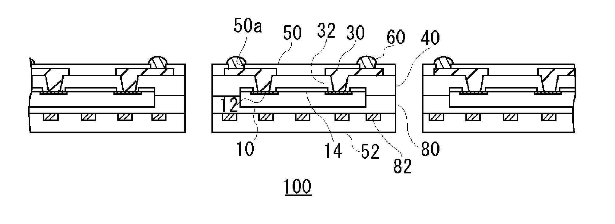
FIG. 1 is a schematic cross-sectional view showing a structure of a semiconductor module 100 according to a first embodiment. The semiconductor module 100 includes, as principal components, a semiconductor device 10, a first insulating resin layer 20, a wiring layer 30, a second insulting resin layer 40, a protective layer 50, an insulating layer 52, and an external connection electrode 60.
The semiconductor device 10 has a device electrode 12 on one of main surfaces, namely on a main surface S11 thereof. Also, a device protective layer 14, in which openings are provided so that the device electrode 12 can be exposed from the openings, is stacked on a main surface S11 side. A specific example of the semiconductor device 10 is a semiconductor chip such as an integrated circuit (IC) or a large-scale integrated circuit (LSI). A specific example of the protective layer 14 is a polyimide layer or the like. For example, aluminum (Al) is used as the device electrode 12.
On ...
second embodiment
(Second embodiment)
In the above-described first embodiment, the semiconductor module 100 is formed in such a manner that the copper sheet 33, on which the bump electrodes are formed as the electrodes 32, and the semiconductor device 10 are press-formed with the second insulating resin layer 40 held between the copper sheet 33 and the semiconductor device 10. The semiconductor module 100 may be formed as follows. A description is hereinbelow given of a second embodiment. Note that the same components as those of the first embodiment are given the same reference numerals and the explanation thereof is omitted as appropriate.
FIGS. 5A to 5F are cross-sectional views showing a process in a method, for forming a wiring layer 30 and connecting electrodes 32 to device electrodes 12, according to the second embodiment. As illustrated in FIG. 5A, a copper sheet 35 as a metallic plate and a plurality of semiconductor devices 10 in a state where the intervals are widened on the first insulating...
third embodiment
(Third embodiment)
A description is hereinbelow given of a third embodiment. Note that the same components as those of the first embodiment are given the same reference numerals and the explanation thereof is omitted as appropriate.
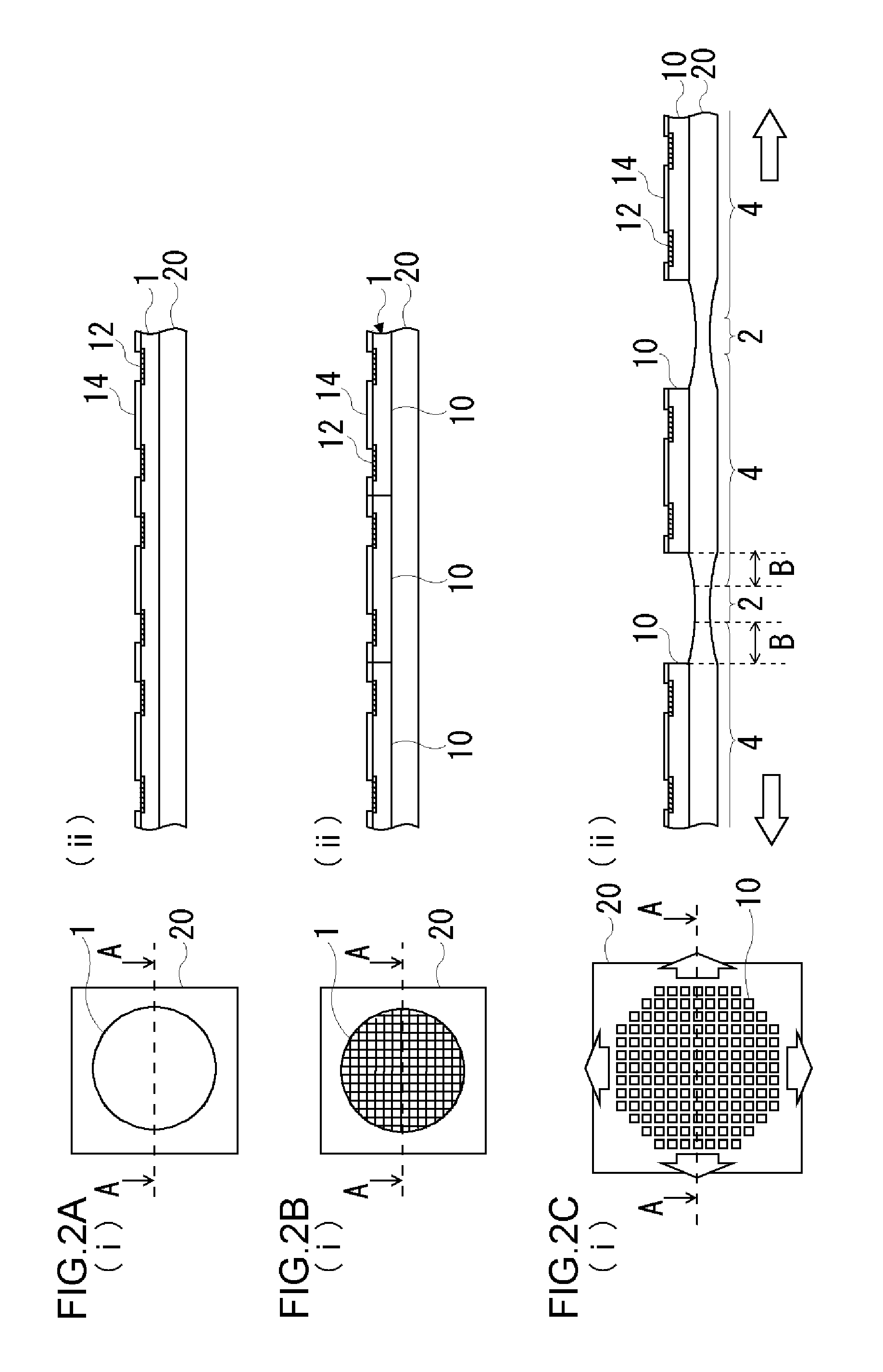
FIGS. 6A to 6C are cross-sectional views showing a process in a method for dicing a semiconductor wafer into a plurality of individual semiconductor devices 10. In each Figure, (i) is a plan view and (ii) is a cross-sectional view taken along the line A-A of (i). In (i) of each Figure, the device electrode 12 shown in (ii) is omitted.
As illustrated in FIG. 6A, prepared first is a semiconductor wafer 1 as a semiconductor substrate where a plurality of semiconductor devices 10 each provided with device electrodes 12 disposed on one main surface S11 thereof are formed and arranged in a matrix shape. The thus prepared semiconductor wafer 1 is bonded onto a first insulating resin layer 20 having an expansibility. In the present embodiment, as will be described ...
PUM
 Abstract
Description
Claims
Application Information