Display panel

US20110199359A1Inactive Publication Date: 2011-08-18GLOBAL OLED TECH

Image

  • Display panel
  • Display panel
  • Display panel

Examples


Embodiment Construction

[0023]A preferred embodiment of the present invention will be described in detail with reference to the accompanying drawings.

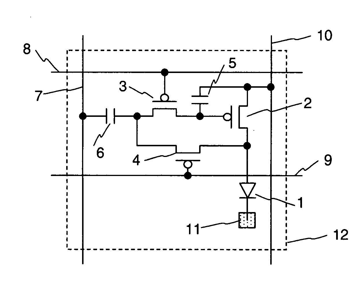
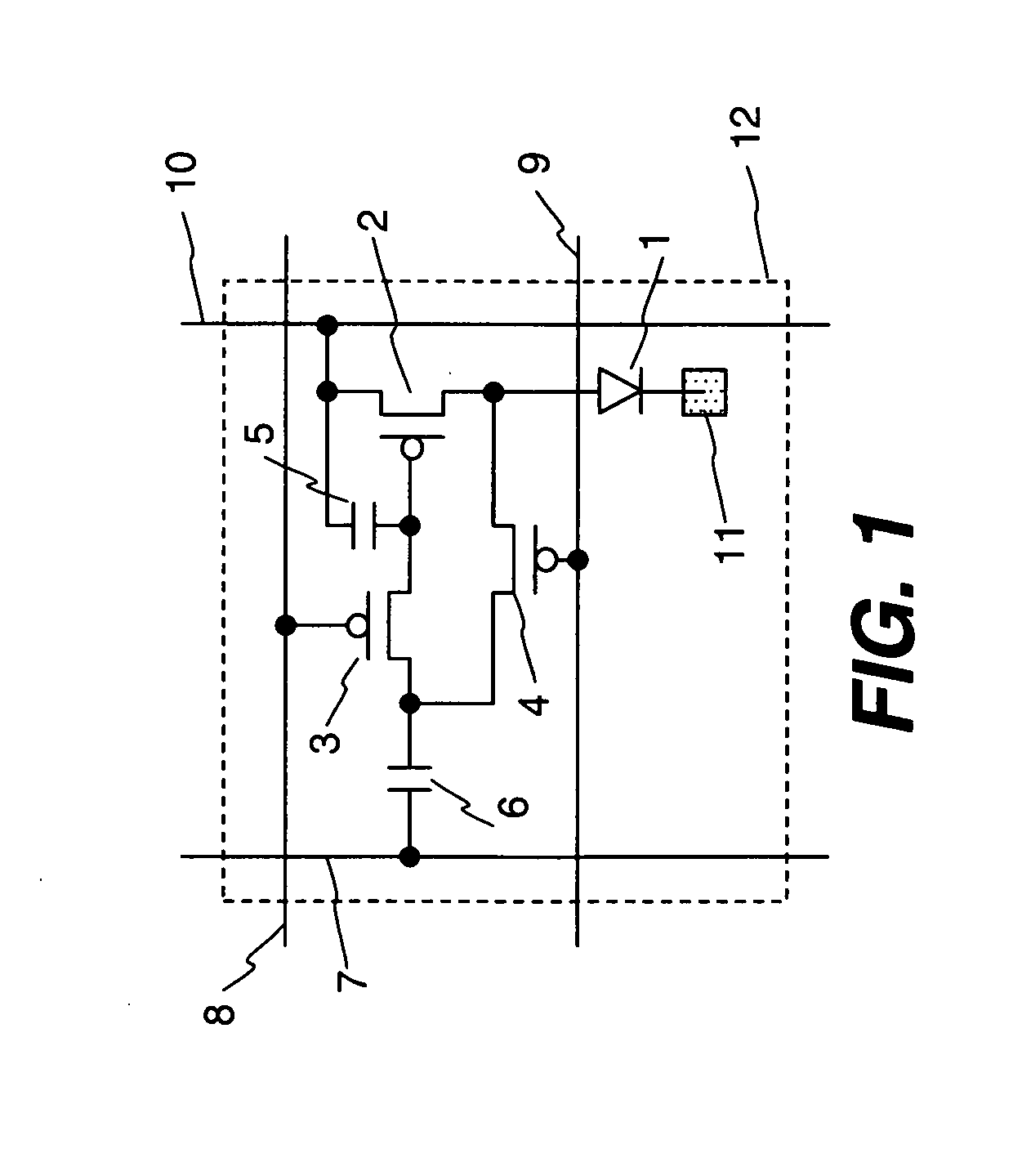
[0024]FIG. 1 shows an example structure of a pixel 12 in a display according to an embodiment of the present invention. The pixel 12 includes an organic EL element 1 which is a light emitting element, a driving transistor 2, a selection transistor 3, a reset transistor 4, a storage capacitor 5, and a coupling capacitor 6. Here, all these transistors are P-type thin film transistors.

[0025]A source terminal of the driving transistor 2 is connected to a power source line 10 which is common for all the pixels. Further, a drain terminal of the driving transistor 2 is connected to an anode of the organic EL element 1 and to a source terminal of the reset transistor 4. A gate terminal of the driving transistor 2 is connected to one terminal of the storage capacitor 5 having the other terminal thereof connected to the power source line 10, and is also connected to a ...


PUM


Abstract

An EL light-emitting element is driven digitally to reduce power consumption using a pixel having three transistors and two capacitors. A reset transistor for diode connection writes the threshold voltage of the drive transistor onto a coupling capacitor. The data voltage plus threshold voltage is then written onto the gate of the drive transistor. This reduces the amplitude of the data voltage required, further reducing power consumption.

Description

FIELD OF THE INVENTION[0001]The present invention relates to a display panel including pixels disposed in a matrix shape.BACKGROUND OF THE INVENTION[0002]Organic EL displays, which are self-emission type displays, are advantageous in high contrast and high-speed response and are therefore suitable for moving image applications such as televisions which display natural images. In general, organic EL elements are driven by using control elements such as transistors, and multi gray level display may be achieved by driving the transistors with a constant current in accordance with data, or by driving the transistors with a constant voltage to vary the light emission period.[0003]Here, with the constant current driving in which the transistors are used in the saturation region, variations in the characteristics of the transistors such as threshold values and mobility would cause a variation in the electric current flowing in the organic EL element, which results in non-uniform display. I...

Claims


Application Information

Patent Timeline
18 Aug 2011
Publication
US20110199359A1
IPC
G09G5/00
CPC
G09G3/3233; G09G2300/0819; G09G3/00; G09G2300/0861; G09G2320/0233; G09G2300/0842; G09G3/2092; G09G2330/021
Inventors
KAWABE, KAZUYOSHI