Wiring substrate and method for manufacturing the same

a technology of wiring substrate and wiring plate, which is applied in the direction of printed circuit manufacturing, printed circuit non-printed electric component association, printed circuit incorporation, etc., can solve the problems of increasing the amount of heat generated by electronic devices, increasing the size of electronic equipment, and generating a particularly large amount of hea

Inactive Publication Date: 2011-08-25
EMPIRE TECH DEV LLC
View PDF2 Cites 26 Cited by
  • Summary
  • Abstract
  • Description
  • Claims
  • Application Information

AI Technical Summary

Benefits of technology

[0013]A method of manufacturing a wiring substrate according to the embodiments disclosed herein includes forming a buffer layer containing a phase change material or a material with an electrocaloric effect so that the buffer layer covers at least a part of a metal core, and mounting an electronic device on a surface of a base including the metal core and the buffer layer or inside the base.

Problems solved by technology

In addition, such electronic equipment has been increasingly miniaturized.
With such improved techniques, the amount of heat generated by electronic devices increases.
However, the heat dissipation capability (heat diffusion capability) of the metal core substrate is still insufficient to apply the metal core substrate to small-sized electronic equipment, which generate a particularly large amount of heat.
This disadvantageously hinders the miniaturization of electronic equipment.

Method used


Image

  • Wiring substrate and method for manufacturing the same
  • Wiring substrate and method for manufacturing the same
  • Wiring substrate and method for manufacturing the same

Examples


Embodiment Construction

[0020]Embodiments disclosed herein will be described below with reference to the figures. In the figures, the same components are denoted by the same reference numerals, and duplicate descriptions are omitted. Furthermore, positional relations such as top and bottom and right and left are based on the illustrated positional relations unless otherwise specified. Moreover, the scaling of the figures is not limited to the illustrated one. In addition, the following embodiments are examples for description of the present disclosure, and the present disclosure is not intended to be limited to the embodiments disclosed herein. Moreover, many variations may be made to the embodiments disclosed herein without departing from the spirit of the present disclosure.

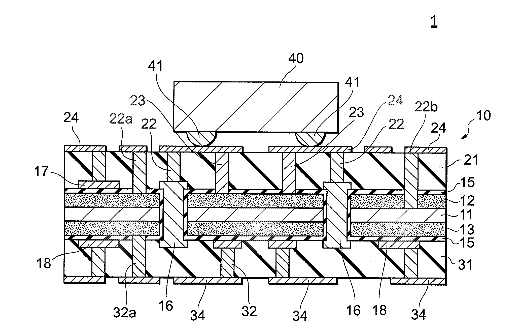
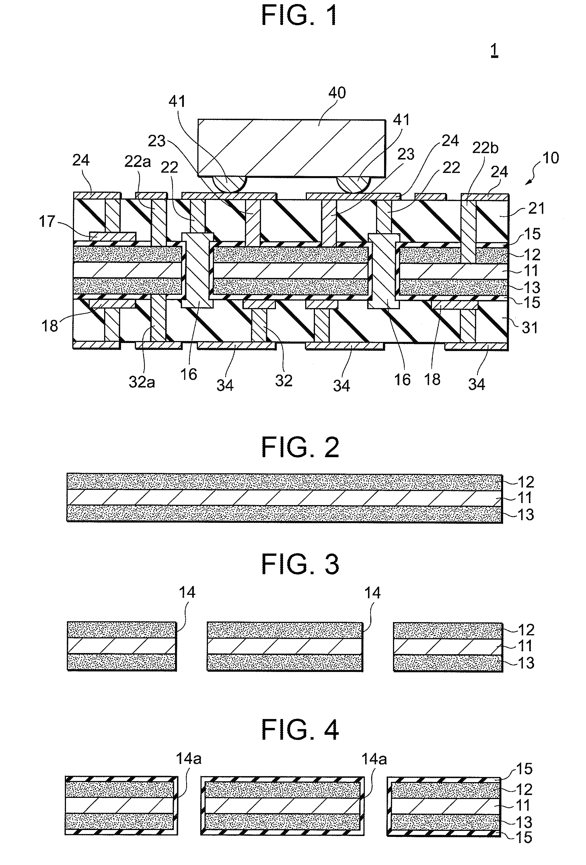
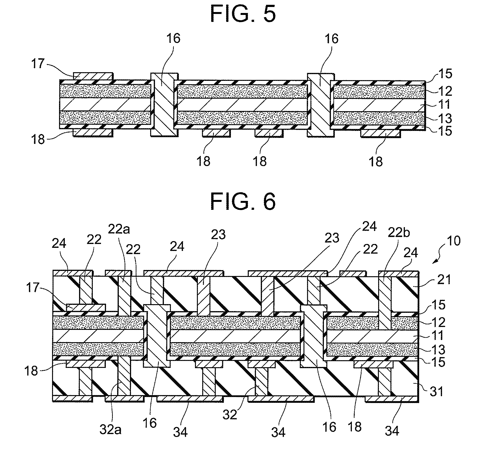
[0021]FIG. 1 is a sectional view showing a wiring substrate 1 according to a first embodiment. The wiring substrate 1 includes a base 10 and an electronic device 40 mounted on a front surface of the base 10.

[0022]The base 10 includes ...


PUM

PropertyMeasurementUnit
thicknessaaaaaaaaaa
melting pointaaaaaaaaaa

Abstract

A wiring substrate with improved heat dissipation capability and with reduced size is disclosed. The wiring substrate includes a metal core substrate, a buffer layer formed so as to cover at least a part of the metal core substrate and containing a phase change material or a material with an electrocaloric effect, an electronic device mounted on a surface of a base including the metal core substrate and the buffer layer or inside the base, and a thermal via formed between the electronic device and the buffer layer.

Description

CROSS-REFERENCE TO RELATED APPLICATIONS[0001]This application claims priority to Japanese Patent Application No. 2010-038398 filed Feb. 24, 2010, which is incorporated herein by reference in its entirety.TECHNICAL FIELD[0002]Embodiments disclosed herein relate to a wiring substrate and a method for manufacturing the wiring substrate.BACKGROUND[0003]The performance of various types of electronic equipment such as mobile phones and personal computers has been improved. In addition, such electronic equipment has been increasingly miniaturized. With such improved techniques, the amount of heat generated by electronic devices increases. Thus, there has been a demand for a new cooling technique for implementing small-sized high-performance equipment.[0004]A technique has been proposed which uses a metal core substrate containing metal with a high heat conductivity instead of a heat sink in order to improve the heat dissipation capability of the electronic equipment without hindering the m...

Claims


Application Information

Patent Timeline
Patent Type & Authority Applications(United States)
IPC IPC(8): H05K1/18H05K1/11H05K3/30
CPCH01L2224/16225H05K1/0206Y10T29/4913H05K3/4608H05K3/445
Inventor IWAMOTO, TAKASHI
Owner EMPIRE TECH DEV LLC
Why Eureka
Try Eureka