

Substrate processing method
a processing method and substrate technology, applied in the field of substrate processing methods, can solve the problems of increasing complexity of processing techniques, increasing the risk of affecting the health of operators, and hygroscopic compounding
Active Publication Date: 2011-08-25
TOKYO ELECTRON LTD
View PDF9 Cites 364 Cited by
- Summary
- Abstract
- Description
- Claims
- Application Information
AI Technical Summary
Benefits of technology
The present invention provides a technique for removing toxic ammonium silicofluoride formed on a substrate by a plasma process, which prevents adverse effects on human bodies. The substrate processing method involves applying a plasma process using a process gas containing fluorine and nitrogen and hydrogen to the substrate, and then heating the substrate at a temperature not less than the decomposition temperature of ammonium silicofluoride in a separate processing vessel. The method can be used in a substrate processing system that includes a plasma processing apparatus and a heating apparatus connected through a vacuum transfer chamber. The computer program of the invention includes steps for practicing the substrate processing method. The technical effect of the invention is to provide a convenient and simple way to remove toxic ammonium silicofluoride from substrates.
Problems solved by technology
Processing techniques have become complicated more and more along with complexification of device structures and miniturization of patterns.
Since the compound is toxic to human bodies, when the substrate is delivered to a working environment outside of the processing apparatus in a state where the compound is deposited on the substrate, this inevitably results in a worry of giving undesired effects on operators' health.
Further, the compound is hygroscopic and may possibly absorb water of a high dielectric constant to increase the dielectric constant of the wafer, as well as it may possibly oxidize barrier metals or interconnection materials.
However, if water or the like used for cleaning intrudes into the SiOCH film, this causes increase of the dielectric constant.
Method used
View moreImage
Smart ImageViewing Examples

Examples
example 1
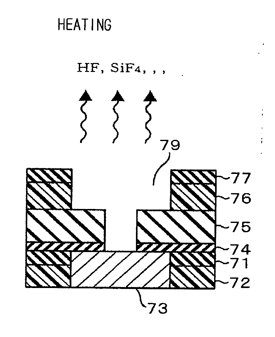
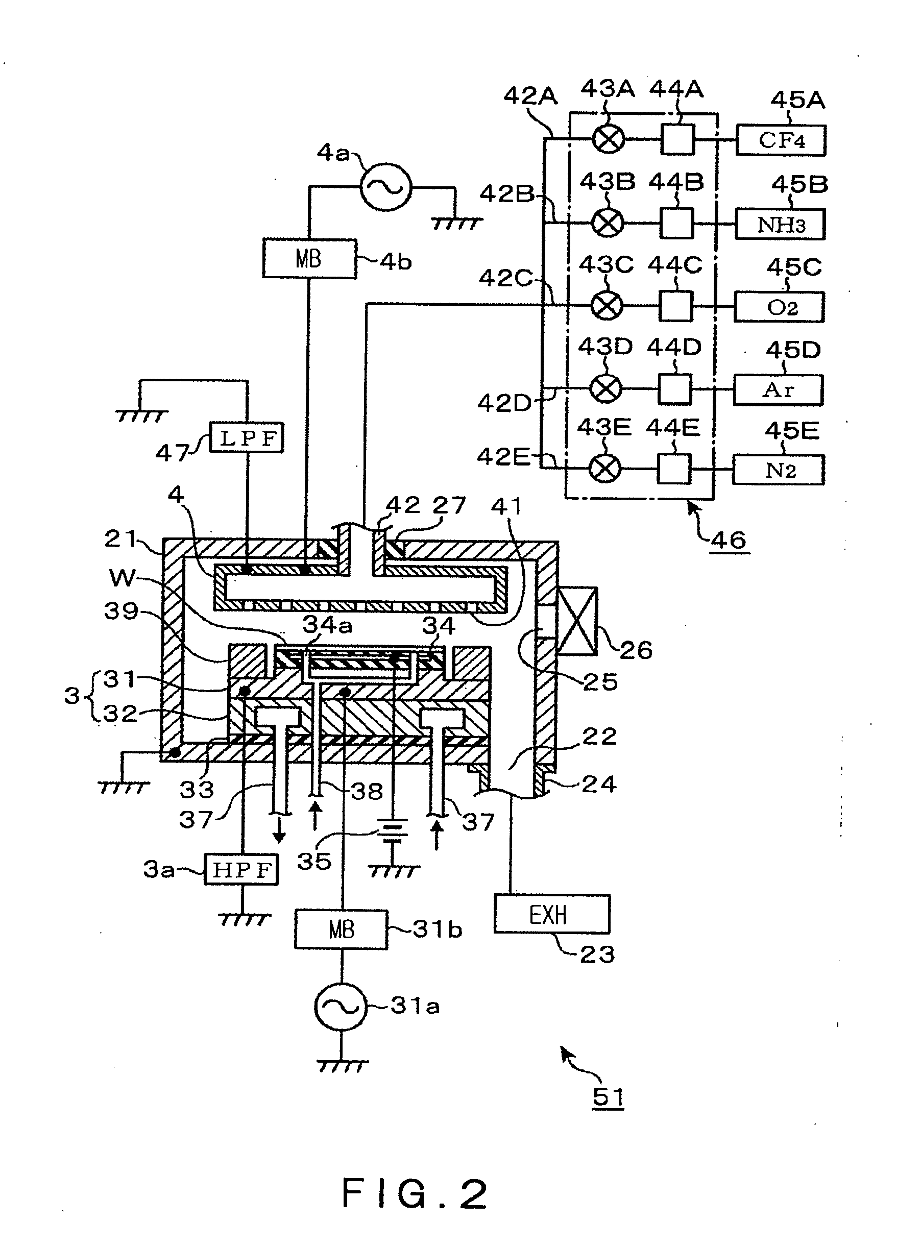
[0080]The etching process for the SiC film 83, the ammonia treatment and the heat treatment described above were applied to a wafer W in accordance with the steps described above.
example 2
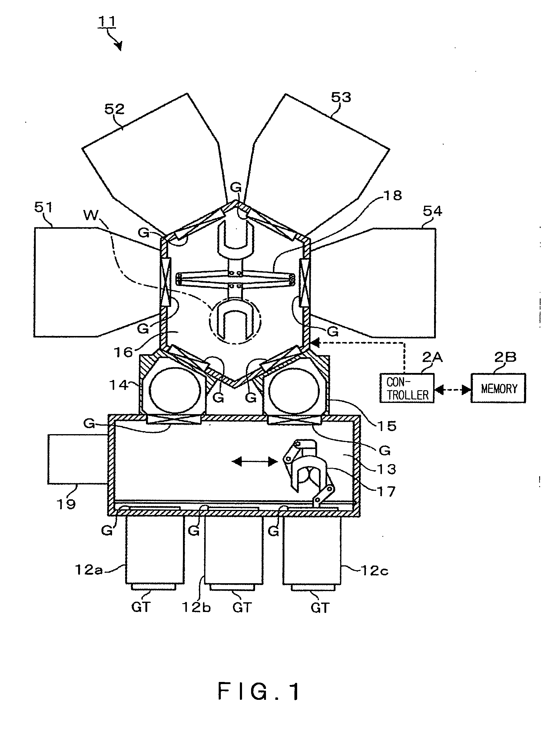
[0081]The same processes as those in Example 1 were applied to a wafer W. In this case, however, for confirming the extent of effects of moisture content in atmospheric air, etching and the ammonia treatment for the SiC film 83 were conducted in the plasma processing apparatus 51, then the wafer W was returned once to the carrier chamber 12a of the surrounding atmosphere, and the wafer W was transported into the heating apparatus 54 and was subjected to the heat treatment.
Login to View More PUM
| Property | Measurement | Unit |
|---|---|---|
| temperature | aaaaa | aaaaa |
| frequency | aaaaa | aaaaa |
| frequency | aaaaa | aaaaa |
Abstract
A silicon-containing film on a substrate is subjected to a plasma process using a process gas containing fluorine and carbon, and is thereafter subjected to plasma process using an ammonia gas, whereby ammonium silicofluoride having toxicity and hygroscopic property is adhered to the substrate. The harmful ammonium silicofluoride is removed by the inventive method. After conducting the plasma process using an ammonia gas, the substrate is heated to a temperature not lower than the decomposition temperature of the ammonium silicofluoride to decompose the ammonium silicofluoride in a process container in which the plasma process was conducted, or in a process container connected with the processing vessel which the plasma process was conducted therein and is isolated from a clean room atmosphere.
Description
CROSS REFERENCE TO RELATED APPLICATION[0001]This application claims the benefit of U.S. provisional application No. 60 / 844,370, which is incorporated herein by reference in its entirety.TECHNICAL FIELD[0002]The present invention relates to a technique of removing ammonium silicofluoride formed on a substrate as a result of conducting a plasma process to the substrate.BACKGROUND ART[0003]Semiconductor device manufacturing includes a process of etching a substrate by using plasma. Processing techniques have become complicated more and more along with complexification of device structures and miniturization of patterns. Accordingly, in many cases, plural kinds of etching gases are used sequentially, for example, in the formation of recesses for burying interconnections and, accordingly, products comprising compounds may be formed on a substrate and such products may remain on the surface of the substrate.[0004]For example, in an etching process of forming recesses for burying Cu interc...
Claims
Login to View More Application Information
Patent Timeline
 Patent Type & AuthorityApplications(United States)
IPC IPC(8): C23F1/02B05D3/10B05D5/00
CPCH01L21/02063H01L21/31116H01L21/67115H01L21/76835H01L21/76807H01L21/76808H01L21/76814H01L21/67201
InventorTAHARA, SHIGERU
OwnerTOKYO ELECTRON LTD