Charge equalizing clock driver and other enhancements for time-of-flight depth sensing and other systems

a clock driver and depth sensing technology, applied in the field of charge equalizing clock driver, can solve the problems of high power dissipation, large total cumulative capacitive load of clock driver, and often consuming substantial operating power of clock driver circuitry, and achieve the effect of substantial capacitive load and substantial operating power loss

Active Publication Date: 2011-08-25
MICROSOFT TECH LICENSING LLC
View PDF2 Cites 17 Cited by
  • Summary
  • Abstract
  • Description
  • Claims
  • Application Information

AI Technical Summary

Benefits of technology

[0020]In one embodiment, an improved clock driver architecture for driving an array of pixel detectors such as found in a TOF system is provided, as is a method for driving such arrays with clock signals. The clock driver preferably outputs first and second complementary clock signals that alternately steer detection photocurrent to different CMOS pixel detectors, whose detection outputs enable measurement of the received image phase or delay. As such, the first and second clock signals see substantial capacitive loading, respectively CL1 and CL2, and, but for the present invention, substantial losses in operating power may exist.

Problems solved by technology

In many applications it is desired to operate TOF systems using battery power, yet TOF clock driver circuitry can often consume substantial operating power.
Each pixel in the array presents a load to the clock driver output, and as a result the total cumulative capacitive load on the clock driver can be quite large.
However the combination of large capacitive clock load and high clock switching rate leads to high power dissipation due to C·V2·f losses, where C is effective capacitive load, V is operating potential, and f is clock frequency.
During time tSC some energy is wasted in each switching transient because useful electrical current flows from power supply V1 to V2, rather than flowing into the load connected to the CMOS inverter output.

Method used


Image

  • Charge equalizing clock driver and other enhancements for time-of-flight depth sensing and other systems
  • Charge equalizing clock driver and other enhancements for time-of-flight depth sensing and other systems
  • Charge equalizing clock driver and other enhancements for time-of-flight depth sensing and other systems

Examples


Embodiment Construction

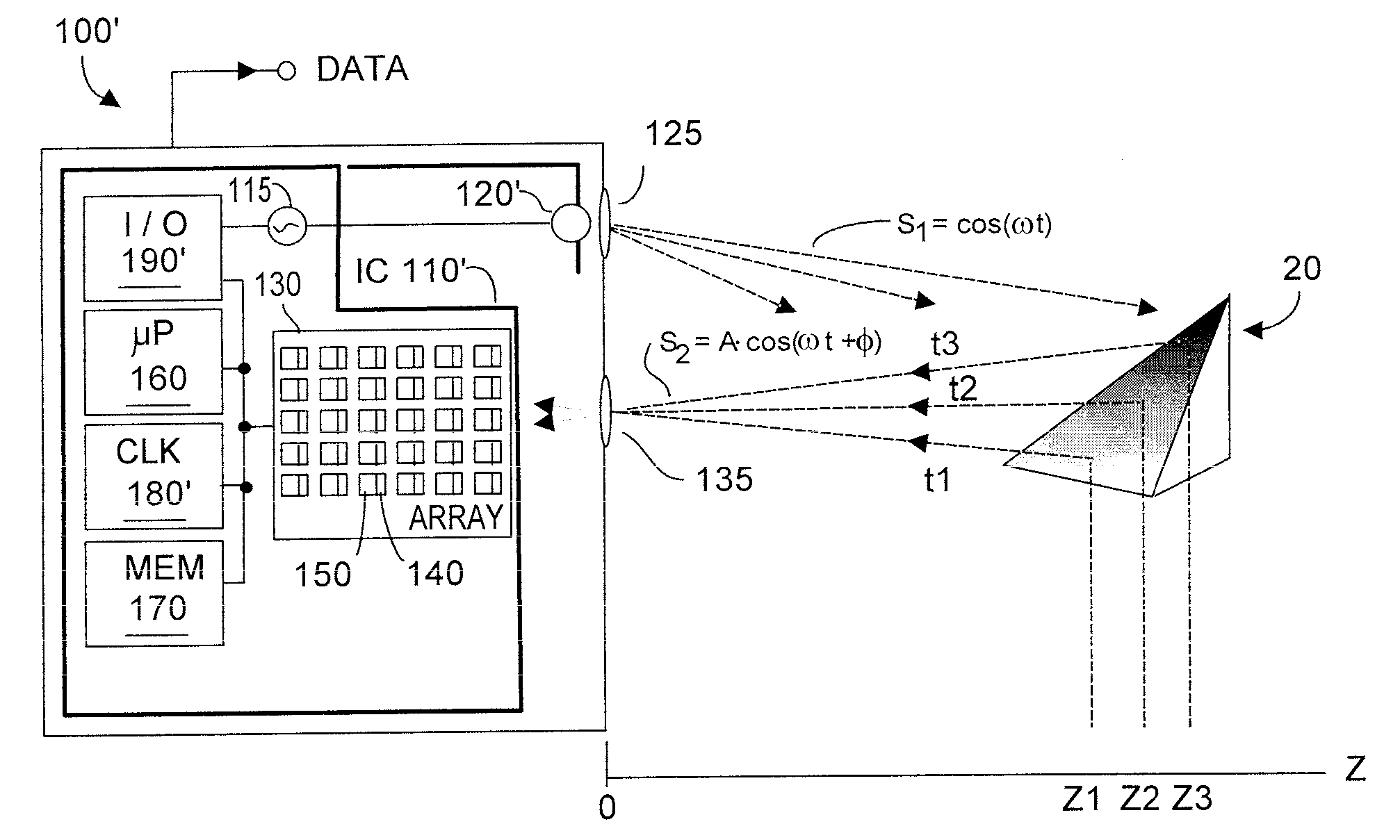
[0045]FIG. 3 depicts a TOF depth system 100′ that is similar to system 100 shown in FIG. 1A, but for components called out with different reference numerals, e.g., clock unit 180′, input / output unit 190′, optionally emitter(s) 120′, and IC 110′. Thus operation of TOF system 100′ is similar or identical to operation of system 100 shown in FIG. 1, but for the improvements described herein.

[0046]In one embodiment, an improved clock driver architecture for driving an array 130 of pixel detectors such as found in a TOF system 100′ is provided, as is a method for driving such arrays. The clock driver may be implemented as part of clock unit 180′ in TOF system 100′ in FIG. 3, and outputs first and second preferably complementary clock signals whose duty cycle is preferably substantially 50%, i.e., square-wave, but may in fact have a duty cycle other than 50%. In a TOF image system application, the first and second clock signals alternately steer detection photocurrent to different CMOS pix...


PUM


Abstract

A clock driver outputs first and second preferably complementary clock signals coupled to substantially equal capacitive loads. Before each clock state change, the clock driver briefly shorts-together the first and second clock signals, to equalize change on capacitive loads, which each assume a potential midway between high and low power supply levels. Charge from the logic high clock signal can thus be used to raise logic low level clock line, and vice versa, rather than draw power supply current. Substantial energy savings on the order of C·V2·f is achieved, where C is effective capacitive load, V is power supply magnitude, and f is clock frequency. The clock driver includes first and second enhanced inverters (inverters that cannot enter short-circuit current mode) whose outputs are the first and second clock signals, and a transistor switch coupled between the inverter outputs. Turning on the transistor switch forces charge equalization.

Description

RELATION TO CO-PENDING APPLICATION[0001]Priority is claimed from co-pending U.S. provisional patent application Ser. No. 61 / 336,311, filed 19 Jan. 2010 and entitled “Low Power Consumption Clock Circuitry, Semiconductor Backside Mirror, and High Power Frequency Laser Unit, and Advanced Filtering Concepts, Useful for Diverse Applications Including Time-of-Flight Depth Sensing”.FIELD OF THE INVENTION[0002]The invention provide a charge equalizing clock driver with reduced power consumption, suitable for driving an array of image sensors in time-of-flight (TOF) imaging sensing systems, among other applications. The invention also provides for optional use of semiconductor backside mirrors, high frequency laser units, and advanced filtering concepts, useful for diverse applications including (TOF) depth sensing.BACKGROUND OF THE INVENTION[0003]Three-dimensional time-of-flight (TOF) systems that provide a measure of distance (Z) from the system to a target object without depending upon lu...

Claims


Application Information

Patent Timeline
Patent Type & Authority Applications(United States)
IPC IPC(8): G01C3/08
CPCG01S7/4816G01S17/89G01S17/08
Inventor SNOW, DANETHOMPSON, BARRY
Owner MICROSOFT TECH LICENSING LLC
Why Eureka
Try Eureka