Structures of and methods of fabricating split gate MIS devices

a technology of split gate and mis device, which is applied in the direction of semiconductor devices, basic electric elements, electrical equipment, etc., can solve the problems of difficult formation of isolation oxide, gate poly, interpol oxide and shield poly inside the trench, and the resistance of split gate structures is mainly limited, so as to reduce forward voltage and shorten the channel length. the effect of the forward voltag

Active Publication Date: 2011-09-01
VISHAY SILICONIX LLC
View PDF6 Cites 16 Cited by
  • Summary
  • Abstract
  • Description
  • Claims
  • Application Information

AI Technical Summary

Benefits of technology

[0007]Embodiments of the present invention implement high density power field effect transistor that avoids the channel mobility problems caused by gate oxide scattering, that exhibits lower forward voltage (Vf) rated at high current; and that shows shorter channel length for faster switching. This invention can apply to DC-DC conversion as a synchronized rectifier transistor.

Problems solved by technology

At high density the resistance of these structures is mainly limited by the epitaxial resistance for a given breakdown voltage.
But due to its complexity the split gate structure is more difficult to manufacture.
Under these conditions difficulties in forming a isolation oxide, gate poly, inter poly oxide and shield poly inside a trench are very challenging.

Method used


Image

  • Structures of and methods of fabricating split gate MIS devices
  • Structures of and methods of fabricating split gate MIS devices
  • Structures of and methods of fabricating split gate MIS devices

Examples


Embodiment Construction

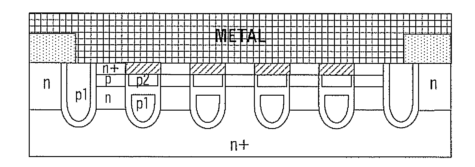
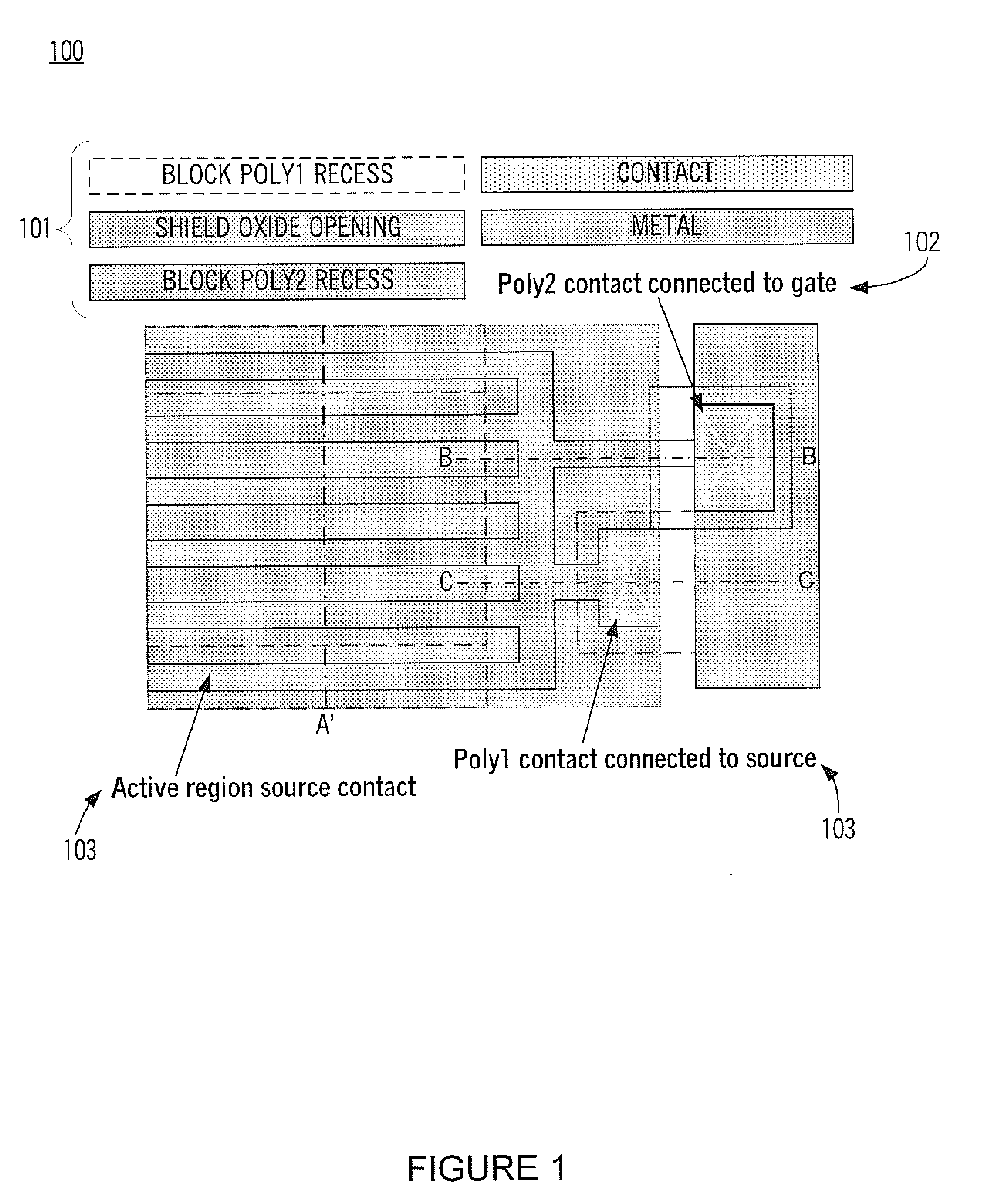
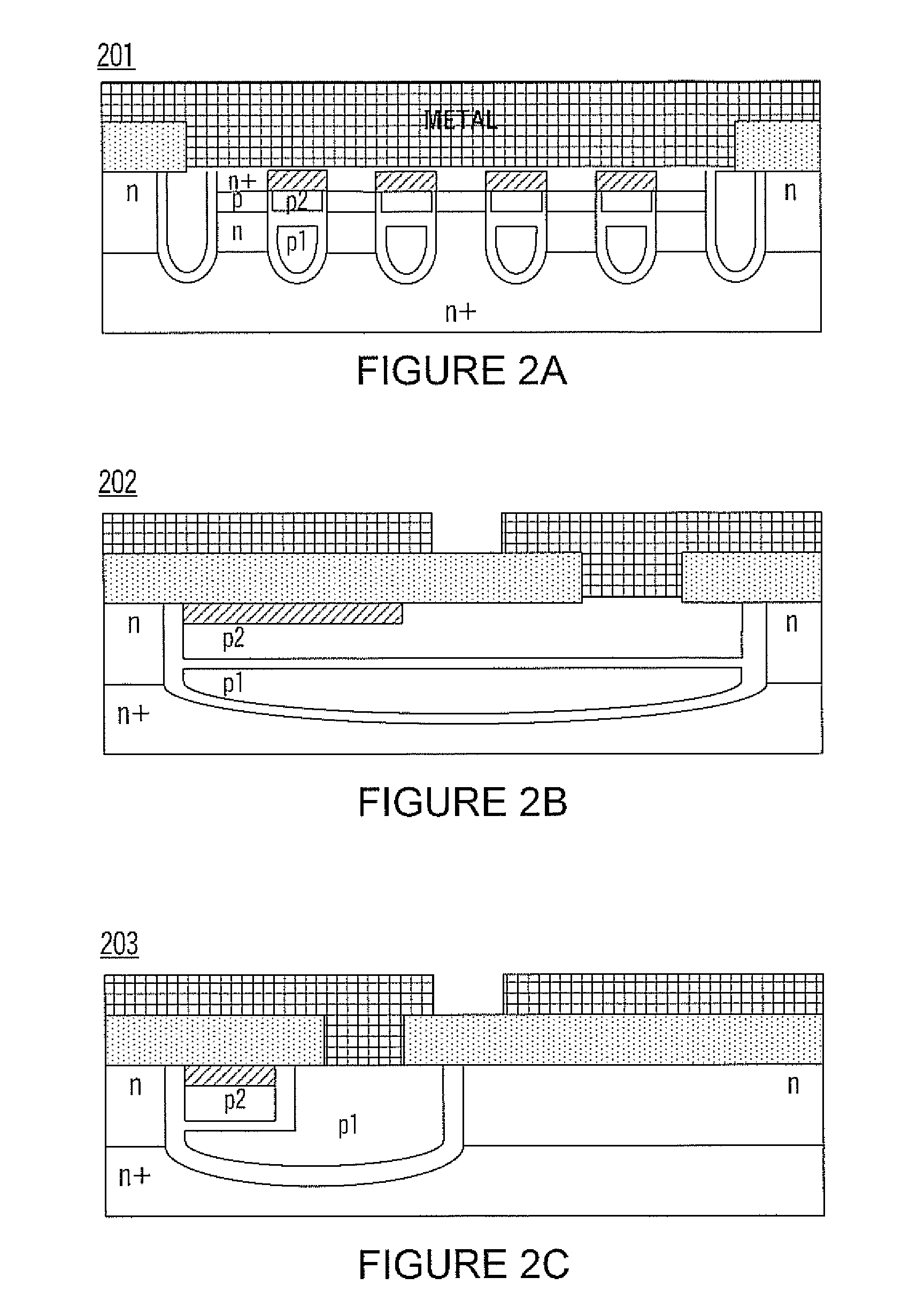
[0040]Reference will now be made in detail to the preferred embodiments of the present invention, examples of which are illustrated in the accompanying drawings. While the invention will be described in conjunction with the preferred embodiments, it will be understood that they are not intended to limit the invention to these embodiments. On the contrary, the invention is intended to cover alternatives, modifications and equivalents, which may be included within the spirit and scope of the invention as defined by the appended claims. Furthermore, in the following detailed description of embodiments of the present invention, numerous specific details are set forth in order to provide a thorough understanding of the present invention. However, it will be recognized by one of ordinary skill in the art that the present invention may be practiced without these specific details. In other instances, well-known methods, procedures, components, and circuits have not been described in detail ...


PUM


Abstract

A split gate field effect transistor device. The device includes a split gate structure having a trench, a gate electrode and a source electrode. A first poly layer is disposed within the trench and is connected to the gate electrode. A second poly layer connected to the source electrode, wherein the first poly layer and the second poly layer are independent.

Description

[0001]This application claims the benefit of U.S. Provisional Patent Application No. 61 / 253,455, filed Oct. 20, 2009, Attorney Docket No. VISH-8792.PRO “STRUCTURES OF AND METHODS OF FABRICATING SPLIT GATE MIS DEVICES”, by Terrill, et al., which is incorporated herein in its entirety.FIELD OF THE INVENTION[0002]The present invention relates to trench MOS transistors.BACKGROUND OF THE INVENTION[0003]Power MOSFETs (metal-oxide-semiconductor field-effect transistors) comprise one of the most useful field effect transistors implemented in both analog and digital circuit applications as energy saving switches.[0004]In general, a trench-based power MOSFET is built using a vertical structure as opposed to a planar structure. The vertical structure enables the transistor to sustain both high blocking voltage and high current.[0005]The conventional trench MOS transistors have realized much higher cell density than the planar MOS transistors. But the denser pitches and the trench structures ha...

Claims


Application Information

Patent Timeline
Patent Type & Authority Applications(United States)
IPC IPC(8): H01L29/772
CPCH01L29/407H01L29/42368H01L29/7813H01L29/66734H01L29/7811H01L29/4238
Inventor TERRILL, KYLEGAO, YANGPARK, CHANHO
Owner VISHAY SILICONIX LLC
Why Eureka
Try Eureka