Methods of forming dual gate of semiconductor device

a dual gate, semiconductor technology, applied in semiconductor/solid-state device manufacturing, basic electric elements, electric apparatus, etc., can solve the problems of gate short circuit and bridging, photoresist residues are not readily removed, and photoresist residues are left behind

Inactive Publication Date: 2011-09-01
SK HYNIX INC
View PDF73 Cites 1 Cited by
  • Summary
  • Abstract
  • Description
  • Claims
  • Application Information

AI Technical Summary

Problems solved by technology

However, the photoresist patterns whose upper portions are hardened due to high concentration ion implantation are incompletely removed by dry stripping using an oxygen plasma, thus leaving photoresist residues behind.
The photoresist residues are not readily removed in the subsequent cleaning and serve as obstacles in the normal implementation of the subsequent gate patterning process, causing many problems, e.g., short circuiting and bridging of gate lines.
In a serious case, the gate conductive layers may remain unetched.
The semiconductor substrate is exposed to air during transfer to a rinse bath or a dryer for rinsing or drying, resulting in the formation of water marks on the surface of the gate conductive layers of p- and n-conductivity types.
The water marks may cause lifting of the gate upon the subsequent gate patterning, and in some cases, they function as etching obstacles so that the gate conductive layers may remain unetched upon gate patterning.

Method used


Image

  • Methods of forming dual gate of semiconductor device
  • Methods of forming dual gate of semiconductor device
  • Methods of forming dual gate of semiconductor device

Examples


Embodiment Construction

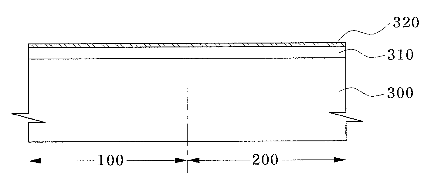
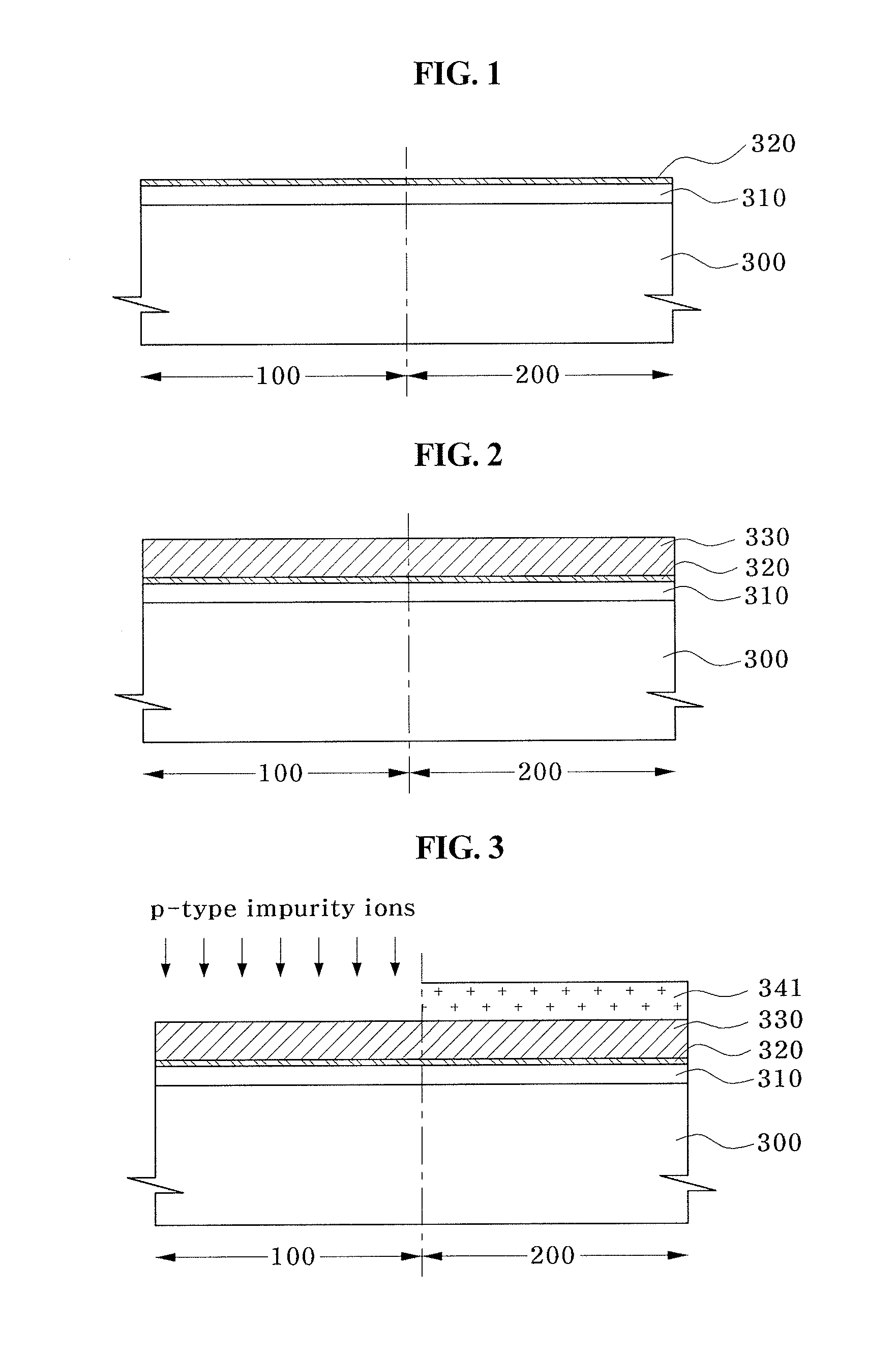
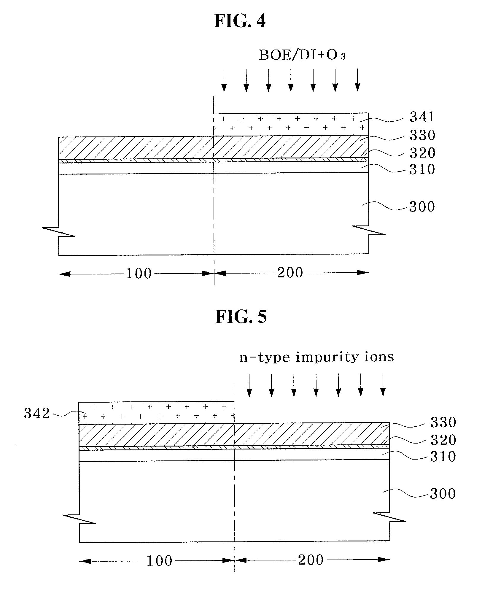
[0022]FIGS. 1 to 9 are cross-sectional views illustrating a method for forming a dual gate of a semiconductor device according to an embodiment of the present invention, FIG. 10 is a diagram showing the structure of a spin-type single cleaner used to remove photoresist residues in methods for forming a dual gate of a semiconductor device according to the present invention, and FIG. 16 shows graphs illustrating a procedure for the removal of a native oxide layer in a method for forming a dual gate of a semiconductor device according to an embodiment of the present invention.

[0023]With reference to FIG. 1, a gate insulating layer 310 is formed on a semiconductor substrate 300 having a first region 100 and a second region 200. The first region 100 is a region where a PMOS transistor is formed, and the second region 200 is a region where an NMOS transistor is formed. The semiconductor substrate 300 is a silicon substrate, but is not limited thereto. For example, the semiconductor substr...


PUM


Abstract

Disclosed herein is a method for forming a dual gate of a semiconductor device. The method comprises the steps of forming a first polysilicon layer doped with p-type impurity ions and a second polysilicon layer doped with n-type impurity ions on a first region and a second region of a semiconductor substrate, respectively, and sequentially subjecting the surfaces of the first and second polysilicon layers to wet cleaning, drying, and dry cleaning. The wet cleaning is performed by using a sulfuric acid peroxide mixture (SPM), a buffered oxide etchant (BOE), and Standard Clean-1 (SC-1) as cleaning solutions.

Description

CROSS-REFERENCES TO RELATED APPLICATIONS[0001]The present application is a divisional of U.S. patent application Ser. No. 11 / 614,975, filed on Dec. 22, 2006, which claims priority to Korean patent application numbers 2005-128307, filed on Dec. 22, 2005, and 2006-88631, filed on Sep. 13, 2006, all of which are incorporated by reference in their entirety.BACKGROUND OF THE INVENTION[0002]1. Field of the Invention[0003]The present invention relates to methods for fabricating a semiconductor device, and more specifically to methods for forming a dual gate consisting of a gate of p-conductivity type and a gate of n-conductivity type in a semiconductor device.[0004]2. Description of Related Art[0005]General complementary metal oxide semiconductor (CMOS) devices have a structure in which a pair of a p-channel type MOS transistor and an n-channel type MOS transistor is formed on one semiconductor substrate so that the transistors operate in a complementary manner. Since this structure of CMO...

Claims


Application Information

Patent Timeline
Patent Type & Authority Applications(United States)
IPC IPC(8): H01L21/20
CPCH01L21/823842H01L21/8238
Inventor KIM, GYU HYUNCHOI, GEUN MINCHOI, II, BAIKKIM, DONG JOOHAN, JI HYE
Owner SK HYNIX INC
Why Eureka
Try Eureka