Touch Sensor Device

Inactive Publication Date: 2011-09-08
FORTREND TAIWAN SCI
View PDF6 Cites 7 Cited by
  • Summary
  • Abstract
  • Description
  • Claims
  • Application Information

AI Technical Summary

Benefits of technology

[0012]Because the touch sensor device according to the present invention has a special single-layer structure, the capacitance of the touch sensor device according to the present invention is greater than that of the conventional touch sensor device. Thus the sensitivity of the touch sensor device according to the present invention is increased

Problems solved by technology

Therefore, there are disadvantages of poor transmittance and thick structure.
Further, because using the optical adhesive 2 to bond the touch penal 3 with the cover lens 1, bubbles are likely to be formed during attaching the touch penal 3 with

Method used


Image

  • Touch Sensor Device
  • Touch Sensor Device
  • Touch Sensor Device

Examples


Embodiment Construction

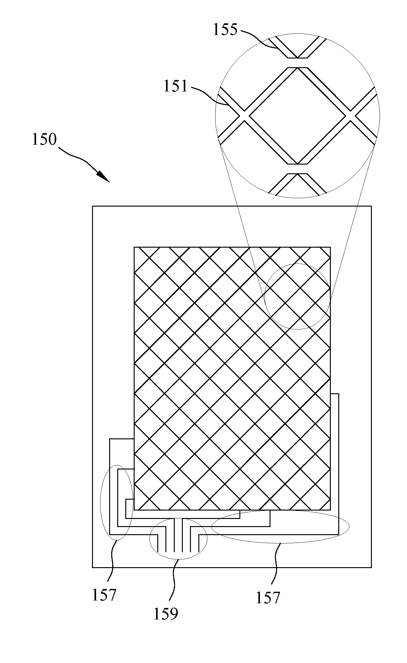
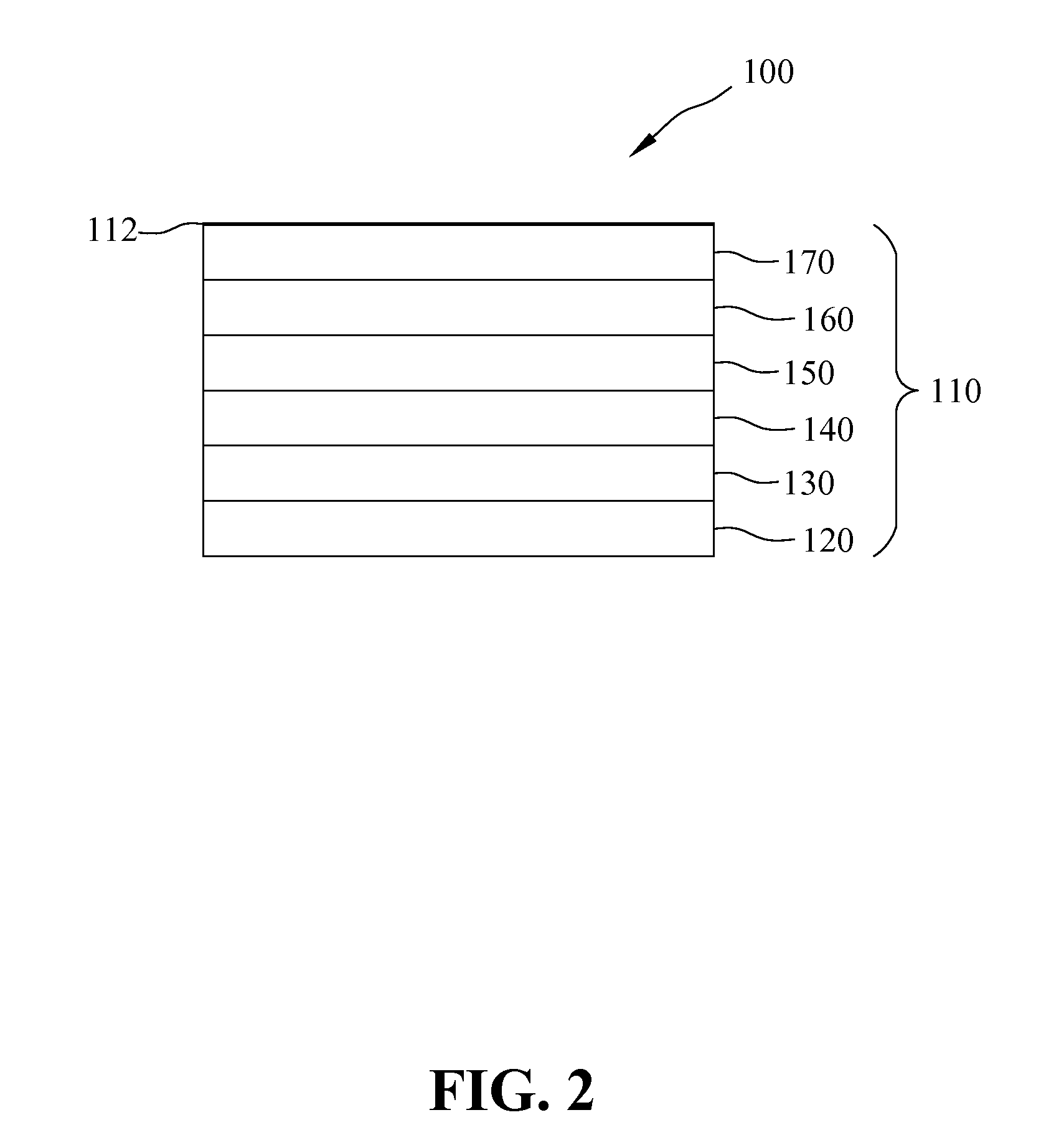
[0021]The accompanying drawings are included to provide a further understanding of the present invention, and are incorporated in and constitute a part of this specification. The drawings illustrate embodiments of the present invention and, together with the description, serve to explain the principles of the present invention.

[0022]Referring to FIG. 2, a touch sensor device 100 according to an embodiment of the present invention includes a substrate 110. The substrate 110, from bottom to top, sequentially includes a bottom conductive layer 120, a bottom insulation layer 130, a top conductive layer 140, an electrode layer 150, a top insulation layer 160 and a substrate material layer 170.

[0023]The substrate 110 has an upper surface 112 for receiving a touch operation. The substrate 110 comprises one of glass and polymethylmethacrylate (PMMA).

[0024]The bottom conductive layer 120 is provided with a shielding effect for shielding any possible external electromagnetic interference, suc...


PUM


Abstract

A touch sensor device with increased transmittance, increased sensitivity and decreased thickness is disclosed. The touch sensor device includes a substrate. The substrate, from bottom to top, sequentially includes a bottom conductive layer, a bottom insulation layer, a top conductive layer, an electrode layer, a top insulation layer and a substrate material layer. The bottom conductive layer can shield external electromagnetic interference and act as a ground. The bottom insulation layer is provided with an insulation effect. The top conductive layer is used for sensing a touch operation to generate a sensor signal. The electrode layer includes a plurality of first electrode lines, a barrier layer and a plurality of second electrode lines. The top insulation layer is provided with an effect for preventing electrostatic discharge. The substrate material layer is used for protecting the touch sensor device.

Description

BACKGROUND OF THE INVENTION[0001]1. Field of the Invention[0002]The present invention is related to a structure of a touch sensor device, and more particularly, to a touch sensor device with increased transmittance, increased sensitivity and decreased thickness which can be manufactured with reduced cost and simplified process.[0003]2. The Prior Arts[0004]Touch sensor devices have been applied widely as user interfaces in various electronic devices, such as cellular phones, tablet computers, personal digital assistants (PDA), and digital home appliances. When in use, users may touch the surface of the touch sensor device by a finger or a touch pen to operate the touch sensor device.[0005]Conventional touch sensor devices are generally formed by bonding a cover lens and a touch panel with an optical clear adhesive (OCA). The touch panel, from bottom to top, sequentially includes a substrate, a bottom insulation layer, a lower conductive layer, a top insulation layer, an electrode lay...

Claims


Application Information

Patent Timeline
IPC IPC(8): G06F3/046H03K17/94G06F3/041
CPCG06F3/041H03K17/94G06F3/046G06F2203/04107G06F3/0446G06F3/0445G06F3/0443G06F2203/04103
Inventor HSIEH, CHAO KUO
Owner FORTREND TAIWAN SCI
Why Eureka
Try Eureka