
Eureka
For R&D, Eureka makes reading and utilizing patents & technical documents easy.
Eureka AIR
Designed for self-driven R&D workflows. Generate viable solutions, solve complex R&D challenges, empower your innovation with AI.

Eureka Materials
Designed for material experts only. Revolutionize your material R&D, from search, analyze, to developing new materials.

TechResearch
Generate reliable direction feasibility study reports for your R&D in just a few steps.

TechSeek
Discover and master advanced knowledge NOW. Basics, ideas, possibilities, all at once.

TechMind
As an expert in R&D Theories, TechMind can generates customized viable solutions instantly.

TechRisk
Analyze your overall solution with one click, know your potential R&D risks in advance.

TechMonitor
Get weekly tech updates, stay abreast of the latest tech innovations and key insights.
Semiconductor device and method for manufacturing semiconductor device
- Summary
- Abstract
- Description
- Claims
- Application Information
AI Technical Summary
Problems solved by technology
Method used
Image

Examples
first embodiment
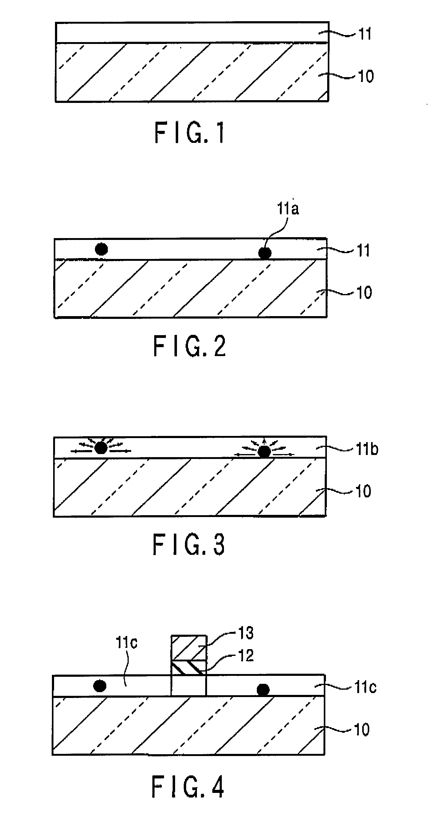
With reference to FIG. 1 to FIG. 4, a method for manufacturing a semiconductor device according to a first embodiment will be described in brief. FIG. 1 to FIG. 4 are sectional views schematically showing a method for forming polycrystalline channel Si in a thin film transistor (TFT).
First, as shown in FIG. 1, an amorphous silicon film 11 that is an amorphous semiconductor film with a thickness of between about 50 nm and about 100 nm is deposited all over a surface of an insulating foundation, specifically a substrate (glass substrate) 10 using SiH4 or Si2H6 or both of these gases. At this time, Ge may be fed into the amorphous silicon film 11 using GeH4 diluted with N2, Ar, or the like. The concentration of Ge is, for example, between about 5% and about 20%. In this case, P, As, In, or the like may be fed.
Then, as shown in FIG. 2, a short-time and high-temperature thermal treatment is carried out, such as milli second annealing (MSA) at a temperature of about 700° C. and about 1,00...
second embodiment
In the above-described first embodiment, microcrystals are formed in an amorphous silicon film, and irradiated with microwaves to form a polycrystalline silicon film. In the second embodiment, a method will be described in which a polycrystalline silicon film is formed by forming microcrystals Ge, forming an amorphous silicon film over the microcrystals Ge, and irradiating the microcrystals with microwaves.
A method for manufacturing a semiconductor device according to the second embodiment will be described in brief with reference to FIG. 18 to FIG. 21. FIG. 18 to FIG. 21 are sectional views schematically showing a method for forming polycrystalline channel Si in a thin film transistor (TFT).
First, as shown in FIG. 18, microcrystals Ge that are microcrystals 41a with a grain size of at most 1 nm are formed on a surface of an insulating foundation, specifically a substrate (glass substrate) 40 by CVD at about 500° C. using GeH4 diluted with N2, Ar, or the like. In this case, the part...
modification 1
(Modification 1)
In the method described above in the second embodiment, microcrystals Ge are formed, and an amorphous silicon film is formed on the microcrystals Ge. Then, the microcrystals are irradiated with microwaves to form a polycrystalline silicon film in the planar structure. In Modification 1 of the second embodiment, a method will be described in which high-quality polycrystal is formed in a hole structure using the method for manufacturing a polycrystalline silicon film according to the embodiment.
A method for manufacturing a semiconductor device according to Modification 1 of the second embodiment will be described in brief with reference to FIG. 22 to FIG. 29. FIG. 22 to FIG. 29 are sectional views schematically showing the method for manufacturing a semiconductor device according to Modification 1 of the second embodiment.
First, as shown in FIG. 22, an SiN stopper film (not shown in the drawings) is formed on an electrode 50 formed of polycrystalline silicon or metal o...
PUM
 Abstract
Description
Claims
Application Information
 - R&D Engineer
- R&D Manager
- IP Professional
- Industry Leading Data Capabilities
- Powerful AI technology
- Patent DNA Extraction
Browse by: Latest US Patents, China's latest patents, Technical Efficacy Thesaurus, Application Domain, Technology Topic, Popular Technical Reports.
© 2024 PatSnap. All rights reserved.Legal|Privacy policy|Modern Slavery Act Transparency Statement|Sitemap|About US| Contact US: help@patsnap.com