Method for manufacturing photoelectric conversion device

a technology of photoelectric conversion device and manufacturing method, which is applied in the direction of radiation controlled device, final product manufacturing, sustainable manufacturing/processing, etc., can solve the problems of insufficient supply of silicon ingots, inability to respond to the expansion of the market, and low productivity, so as to reduce the rate of deterioration of characteristics by light deterioration and high quality

Inactive Publication Date: 2009-02-19
SEMICON ENERGY LAB CO LTD
View PDF33 Cites 60 Cited by
  • Summary
  • Abstract
  • Description
  • Claims
  • Application Information

AI Technical Summary

Benefits of technology

[0013]According to the present invention, a semi-amorphous semiconductor with high quality can be obtained without reducing the deposition rate. By forming a photoelectric conversion layer using such a semi-amorphous semiconductor, a rate of deterioration in characteristics by light deterioration is decreased from one-fifth to one-tenth, and thus, a photoelectric conversion device that has almost no problems for practical use can be obtained. Since a rate

Problems solved by technology

However, it takes a long time to manufacture large silicon ingots, which means productivity is low, and since supply of raw materials of silicon itself is limited, the supply of silicon ingots is insufficient and cannot respond to the expansion of the market.
However, light deterioration is not overcome, and thus the photoelectric conversion devices using amorphous silicon do not spread.
However, light deterioration called Staebler-Wronski effect can not be overcome.
In order to form a photoelectric conversion layer us

Method used


Image

  • Method for manufacturing photoelectric conversion device
  • Method for manufacturing photoelectric conversion device
  • Method for manufacturing photoelectric conversion device

Examples


embodiment mode 1

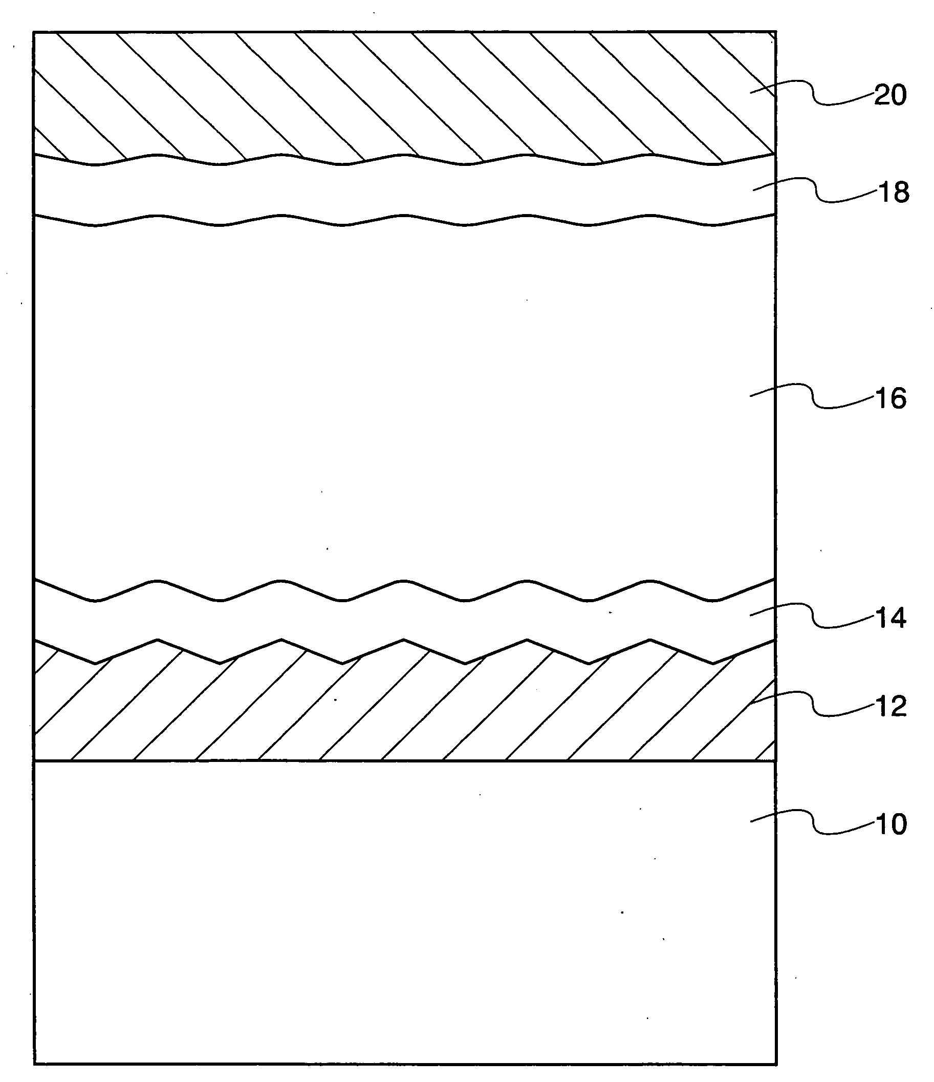
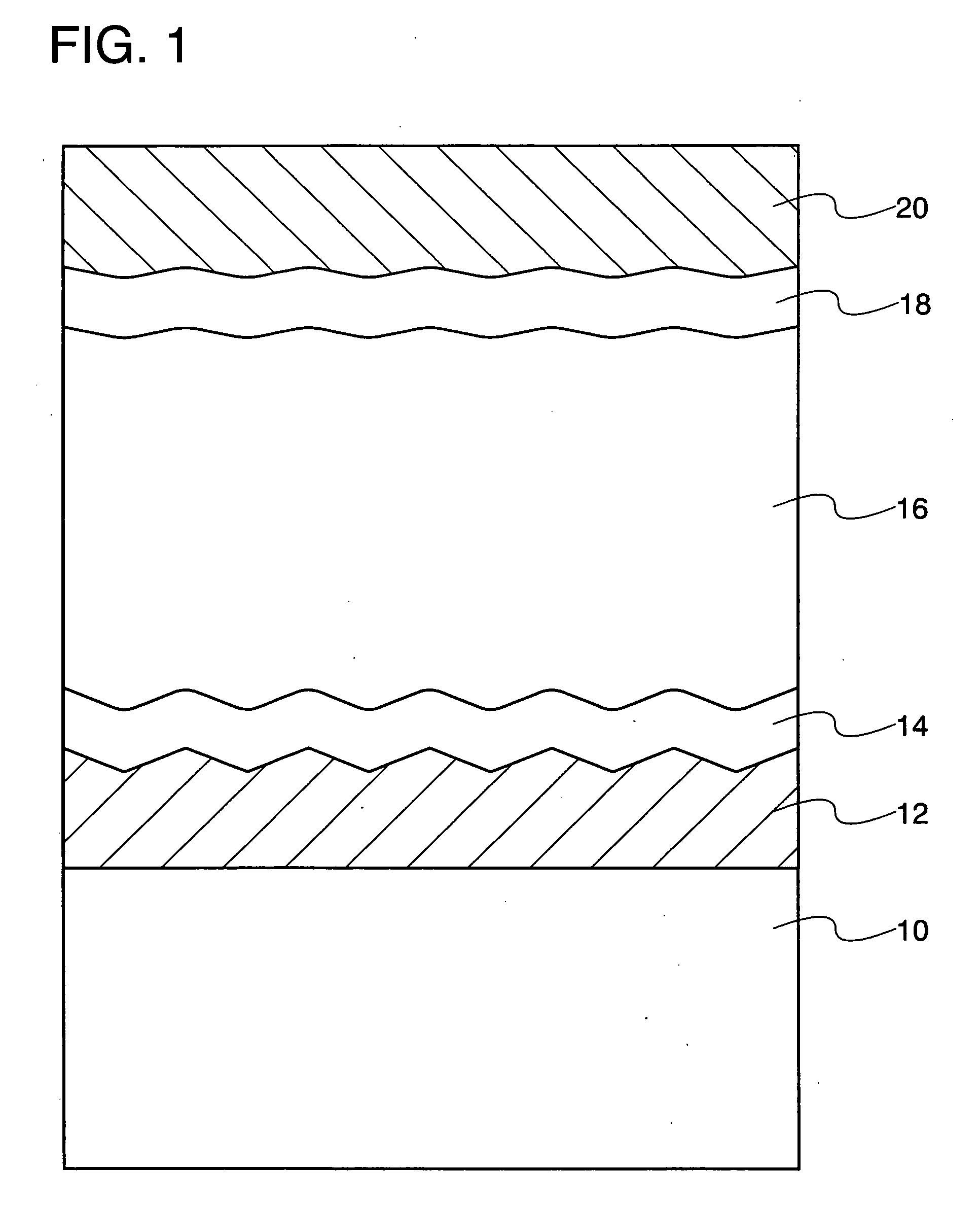
[0040]FIG. 1 shows a structure of a photoelectric conversion device according to this embodiment mode. This photoelectric conversion device includes at least one semiconductor junction by providing an i-type semiconductor layer 16 interposed between a p-type semiconductor layer 14 and an n-type semiconductor layer 18. In this embodiment mode, a layer including the p-type semiconductor layer 14, the n-type semiconductor layer 18, and the i-type semiconductor layer 16, in other words, a photoelectric conversion layer, is formed using a semi-amorphous semiconductor layer.

[0041]A substrate 10 can be formed using various commercial glass plates such as soda-lime glass, lead glass, strengthened glass, and ceramic glass. Further, a non-alkali glass substrate such as an aluminoborosilicate glass substrate or a barium borosilicate glass substrate, a quartz substrate, or a metal substrate such as a stainless steel substrate can be used. In a case where light enters from the substrate 10 side,...

embodiment mode 2

[0115]FIG. 11A shows a structure of a photoelectric conversion device according to this embodiment mode. In this photoelectric conversion device, an i-type semiconductor layer 16 is provided between a p-type semiconductor layer 14 and an n-type semiconductor layer 18, whereby at least one semiconductor junction is included. A layer including the p-type semiconductor layer 14, the n-type semiconductor layer 18, and the i-type semiconductor layer 16, that is, a photoelectric conversion layer, is formed of a semi-amorphous semiconductor layer.

[0116]A substrate 10 can be various glass substrates described in Embodiment Mode 1. In a case where light enters from the substrate 10 side, a first electrode 12 can be formed of a transparent conductive material such as indium oxide, indium tin oxide, or zinc oxide as described in Embodiment Mode 1. On the other hand, in a case where the first electrode 12 is a reflective electrode, the first electrode 12 can be formed of a metal material such a...


PUM

PropertyMeasurementUnit
Pressureaaaaaaaaaa
Pressureaaaaaaaaaa
Energyaaaaaaaaaa

Abstract

It is an object to form a high-quality crystalline semiconductor layer directly over a large-sized substrate with high productivity without reducing the deposition rate and to provide a photoelectric conversion device in which the crystalline semiconductor layer is used as a photoelectric conversion layer. A photoelectric conversion layer formed of a semi-amorphous semiconductor is formed over a substrate as follows: a reaction gas is introduced into a treatment chamber where the substrate is placed; and a microwave is introduced into the treatment chamber through a slit provided for a waveguide that is disposed in approximately parallel to and opposed to the substrate, thereby generating plasma. By forming a photoelectric conversion layer using such a semi-amorphous semiconductor, a rate of deterioration in characteristics by light deterioration is decreased from one-fifth to one-tenth, and thus a photoelectric conversion device that has almost no problems for practical use can be obtained.

Description

BACKGROUND OF THE INVENTION[0001]1. Field of the Invention[0002]The present invention relates to a method for manufacturing crystal-system silicon, and also relates to a photoelectric conversion device having a semiconductor junction using the crystal-system silicon and a method for manufacturing the photoelectric conversion device.[0003]2. Description of the Related Art[0004]In response to global environmental issues in recent years, the market for photoelectric conversion devices such as residential photovoltaic systems has expanded. As photoelectric conversion devices, devices using a high conversion efficiency single crystalline or polycrystalline silicon wafer have been used in practice. The photoelectric conversion devices using single crystalline or polycrystalline silicon are manufactured by being cut out of large silicon ingots. However, it takes a long time to manufacture large silicon ingots, which means productivity is low, and since supply of raw materials of silicon it...

Claims


Application Information

Patent Timeline
IPC IPC(8): H01L31/18
CPCC23C16/24H01L31/046H01L21/0237H01L21/02532H01L21/0262H01L21/02678H01L21/67207H01L27/14632H01L31/022425H01L31/022466H01L31/03921H01L31/0745H01L31/075H01L31/18H01L31/1824H01L31/1884Y02E10/545Y02E10/548C23C16/511H01L31/0463H01L31/0465Y02P70/50H01L31/04
Inventor YAMAZAKI, SHUNPEIARAI, YASUYUKI
Owner SEMICON ENERGY LAB CO LTD
Why Eureka
Try Eureka