Photovoltaic device and manufacturing method thereof

a photovoltaic device and manufacturing method technology, applied in the direction of sustainable manufacturing/processing, instruments, final product manufacturing, etc., can solve the problems of adversely affecting the p-n junction characteristics or bsf effect, and it is difficult to completely remove water or organic matter from the surface of the substra

Inactive Publication Date: 2003-09-11
SANYO ELECTRIC CO LTD
View PDF1 Cites 60 Cited by
  • Summary
  • Abstract
  • Description
  • Claims
  • Application Information

AI Technical Summary

Problems solved by technology

Therefore, good interface characteristics can be achieved even with an impure substrate, which is subject to an adverse effect of impurity or deficiency of oxygen induction under a high temperature process.
Because of this low temper...

Method used


Image

  • Photovoltaic device and manufacturing method thereof
  • Photovoltaic device and manufacturing method thereof
  • Photovoltaic device and manufacturing method thereof

Examples


first embodiment

[0034] (First Embodiment)

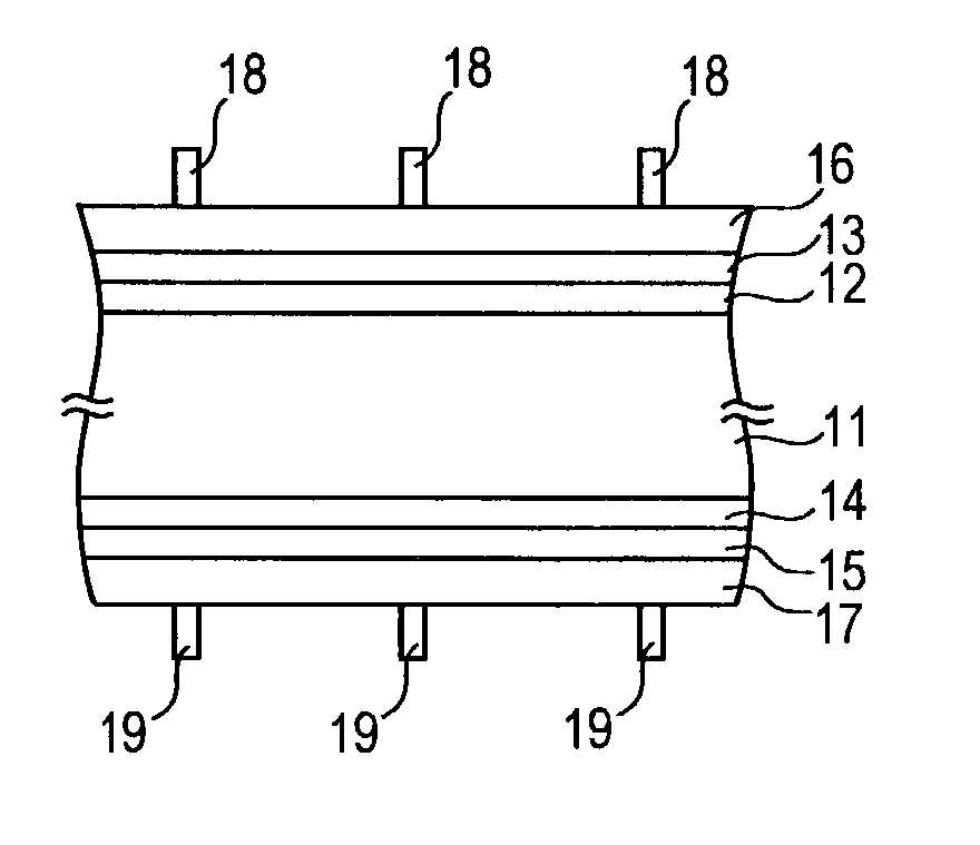
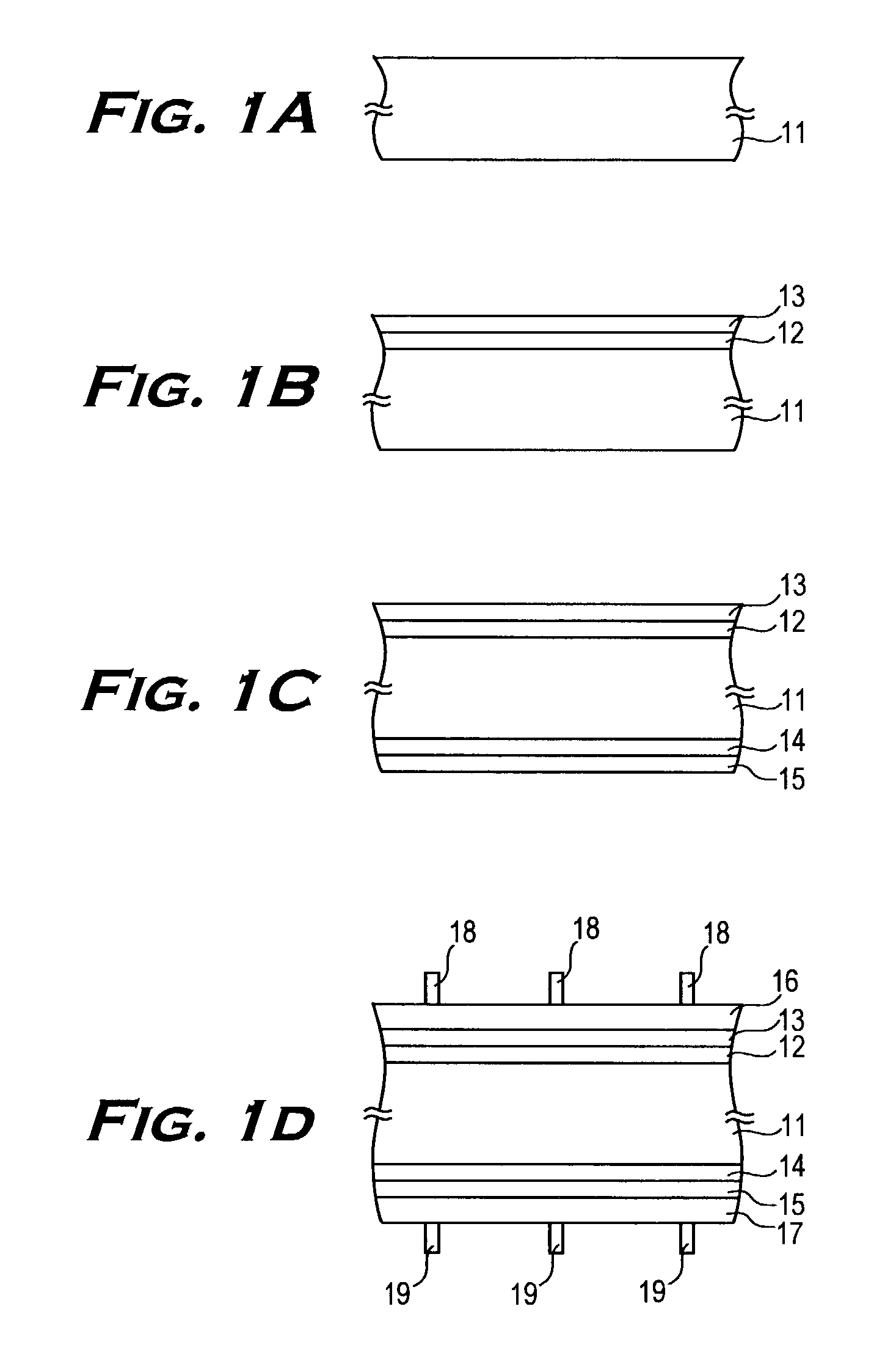
[0035] FIGS. 1A to 1D are cross sectional views illustrating manufacturing processes of a photovoltaic device according to the first embodiment.

[0036] A single crystalline silicon substrate or a polycrystalline silicon substrate may be used as a crystalline semiconductor substrate. In this embodiment, an n-type single crystalline substrate 11 of resistivity not more than 5 .OMEGA.cm and 300 .mu.m in thickness is used. Both front and rear surfaces of this single crystalline silicon substrate 11 are textured by anisotropic etching using alkaline solution such as sodium hydroxide solution or potassium hydroxide solution.

[0037] The single crystalline silicon substrate 11 is cleaned and put into a vacuum chamber to be heated up to not more than 200 degrees centigrade so that water attached to the front surface of the substrate can be removed to the utmost. In this embodiment, the substrate is heated up to 170 degrees centigrade.

[0038] Next, hydrogen gas (H.sub.2)...

second embodiment

[0056] (Second Embodiment)

[0057] Next, explanations are made of the second embodiment. A single crystalline silicon substrate is cleaned and put into a vacuum chamber to be heated up to not more than 200 degrees centigrade so that water attached to a front surface of the substrate can be removed to the utmost. In this embodiment, the substrate is heated up to 170 degrees centigrade.

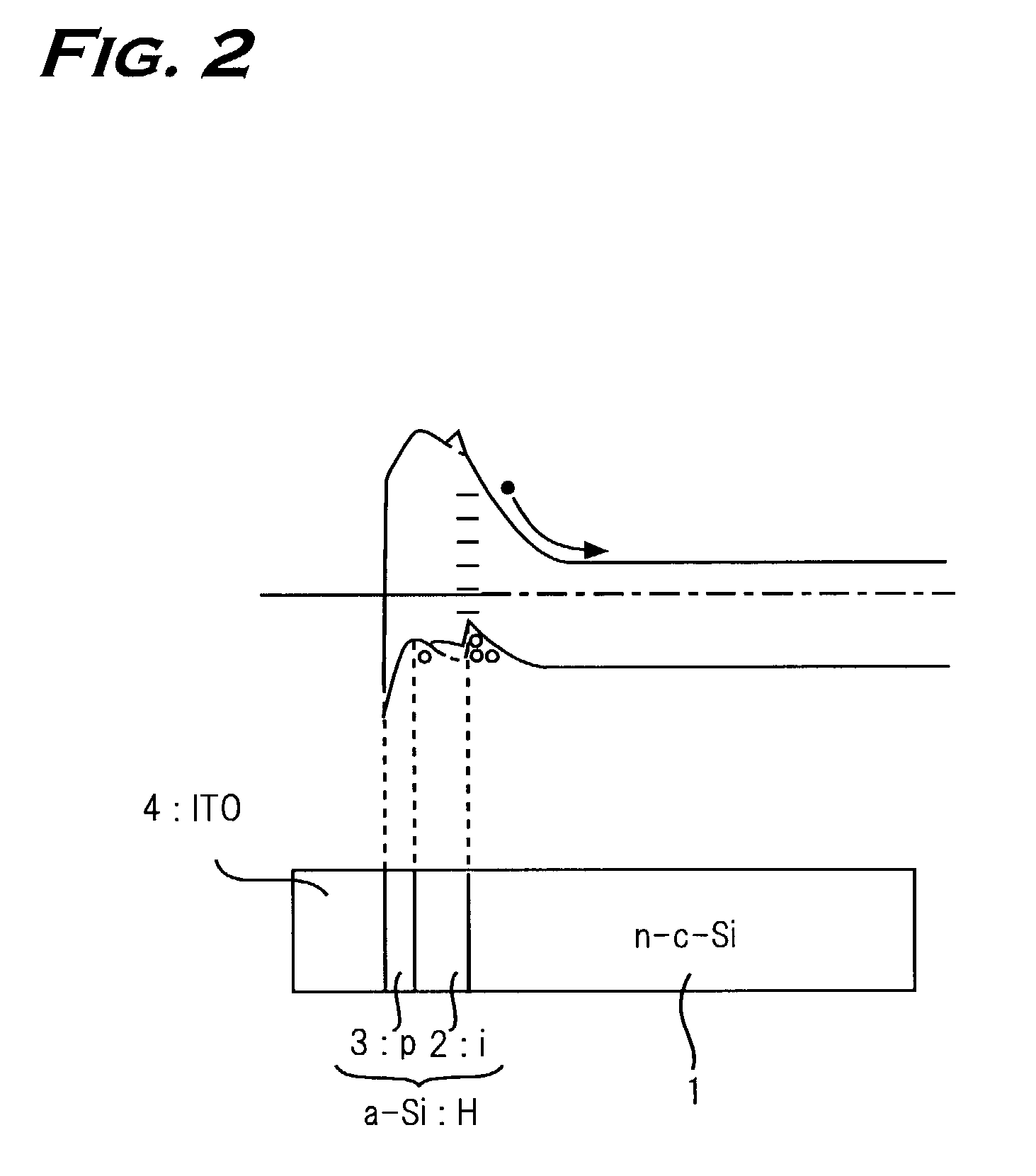
[0058] Next, hydrogen gas (H.sub.2) is introduced and the substrate is exposed to plasma discharge to clean the surface thereof. Then, hydrogen gas (H.sub.2), diborane gas (B.sub.2H.sub.6), silane gas (SiH.sub.4) are introduced and the substrate is exposed to plasma discharge to laminate on the front surface of the substrate a first amorphous silicon layer {circle over (1)} of thickness about 1 nm doped with a slightly p-type impurity of low density so that boron is introduced in the vicinity of an interface. After that, a p-n junction is formed by laminating an i-type amorphous silicon layer {circle over...

third embodiment

[0062] (Third Embodiment)

[0063] Now explanations are made of the third embodiment. A single crystalline silicon substrate is cleaned and put into a vacuum chamber to be heated up to not more than 200 degrees centigrade so that water attached to a front surface of the substrate can be removed to the utmost. In this embodiment, the substrate is heated up to 170 degrees centigrade.

[0064] Next, hydrogen gas (H.sub.2) is introduced and the substrate is exposed to plasma discharge to clean the surface thereof. Hydrogen gas (H.sub.2) and diborane gas (B.sub.ZH.sub.6) are introduced, and the substrate is exposed to said gases. Diborane gas (B.sub.2H.sub.6) is decomposed on and attaches to the heated surface of the substrate so that boron can be introduced in an interface. The substrate is exposed under the condition of substrate temperature of 170 degrees centigrade, density and flow rate of diborane gas (B.sub.2H.sub.6) 2% and 1000 sccm respectively, pressure 40 Pa and treating time 1-600 ...


PUM

PropertyMeasurementUnit
Digital informationaaaaaaaaaa
Temperatureaaaaaaaaaa

Abstract

The present invention was made to improve interface characteristics between a crystalline semiconductor and an amorphous semiconductor thin film so that junction characteristics can be upgraded. A manufacturing method of a photovoltaic device comprising an i-type amorphous silicon thin film (12) and a p-type amorphous silicon thin layer (13) laminated in this order on a front surface of an n-type single crystalline silicon substrate (11), and an i-type amorphous silicon layer (14) and an n-type amorphous silicon layer (15) laminated in this order on a rear surface of the single crystalline silicon substrate, wherein an i-type amorphous silicon layer (12) is formed after the front surface of the single crystalline silicon substrate (11) is exposed to a plasma discharge using mixed gas of hydrogen gas and a gas containing boron so that atoms of boron may be interposed on an interface between the single crystalline silicon substrate (11) and the i-type amorphous silicon layer (12).

Description

[0001] 1. Field of the Invention[0002] This invention relates to a photovoltaic device utilizing hetero semiconductor junction and a manufacturing method thereof.[0003] 2. Description of Prior Art[0004] A photovoltaic device is generally categorized into single crystalline-, polycrystalline-, and amorphous-based type depending on a type of a semiconductor of a part for converting absorbed light mainly into electric current. By the way, a hybrid type photovoltaic device taking both advantages of an amorphous semiconductor thin film and a crystalline semiconductor is studied (JP, H04-130671, A). In this photovoltaic device, an intrinsic amorphous silicon thin film without dopant of a conductive impurity or a substantially intrinsic amorphous silicon thin film doped with a small amount of an element in 3B group of the periodic table such as boron is interposed on a junction interface in forming semiconductor junction by combining a crystalline silicon semiconductor and an amorphous sil...

Claims


Application Information

Patent Timeline
IPC IPC(8): H01L31/04C23C16/24H01L31/06H01L31/0747H01L31/075H01L31/18H01L31/20
CPCH01L31/0747H01L31/075Y02E10/547Y02E10/548H01L31/202Y02P70/50
Inventor TAGUCHI, MIKIOASAUMI, TOSHIOTERAKAWA, AKIRA
Owner SANYO ELECTRIC CO LTD
Why Eureka
Try Eureka