Semiconductor device manufacturing with amorphous film cyrstallization using wet oxygen

a technology of amorphous film and manufacturing method, which is applied in the direction of after-treatment details, crystal growth process, radiation controlled devices, etc., can solve the problems of deteriorating the drivability of thin film transistors, high cost, and extremely irregular surface of polycrystalline silicon films

Inactive Publication Date: 2001-12-11
SANYO ELECTRIC CO LTD
View PDF29 Cites 57 Cited by
  • Summary
  • Abstract
  • Description
  • Claims
  • Application Information

AI Technical Summary

Problems solved by technology

When solid-phase epitaxy of the amorphous silicon film is made in an atmosphere of inert gas such as nitrogen gas, however, the surface of the polycrystalline silicon film is extremely irregularized.
When such a polycrystalline silicon film is employed as an active layer of a thin film transistor, carriers are disadvantageously scattered by the irregular surface of the polycrystalline silicon film, to deteriorate drivability of the thin film transistor.
In order to carry out the mechanical or chemical polishing, however, an expensive machine is necessary and sufficient care is required for maintenance/management of the polishing machine for continually maintai...

Method used


Image

  • Semiconductor device manufacturing with amorphous film cyrstallization using wet oxygen
  • Semiconductor device manufacturing with amorphous film cyrstallization using wet oxygen
  • Semiconductor device manufacturing with amorphous film cyrstallization using wet oxygen

Examples


second experimental example

This Experimental Example is different from first Experimental Example in a point that a high-temperature heat treatment was performed in an N.sub.2 atmosphere after solid-phase epitaxy.

First, an amorphous silicon film was formed on a quartz glass substrate by LP-CVD under film forming conditions shown in Table 6.

Then, an amorphous silicon film was epitaxially grown in a solid phase under the heat treatment conditions shown in Table 2, with employment of the apparatus shown in FIG. 10. Oxygen and wet oxygen which was prepared by the wet oxygen generator were mixed with each other in the flow rates shown in Table 2, and introduced into the silica tube 61.

Further, the interior of the silica tube 61 was heated along the temperature profile shown in FIG. 11, and kept in the heated state when the substrate temperature reached 600.degree. C., to make solid-phase epitaxy for 20 hours. Thereafter a heat treatment was performed in an N.sub.2 atmosphere at a temperature of 1050.degree. C. for...

third embodiment

A third embodiment according to the second aspect of the present invention is now described.

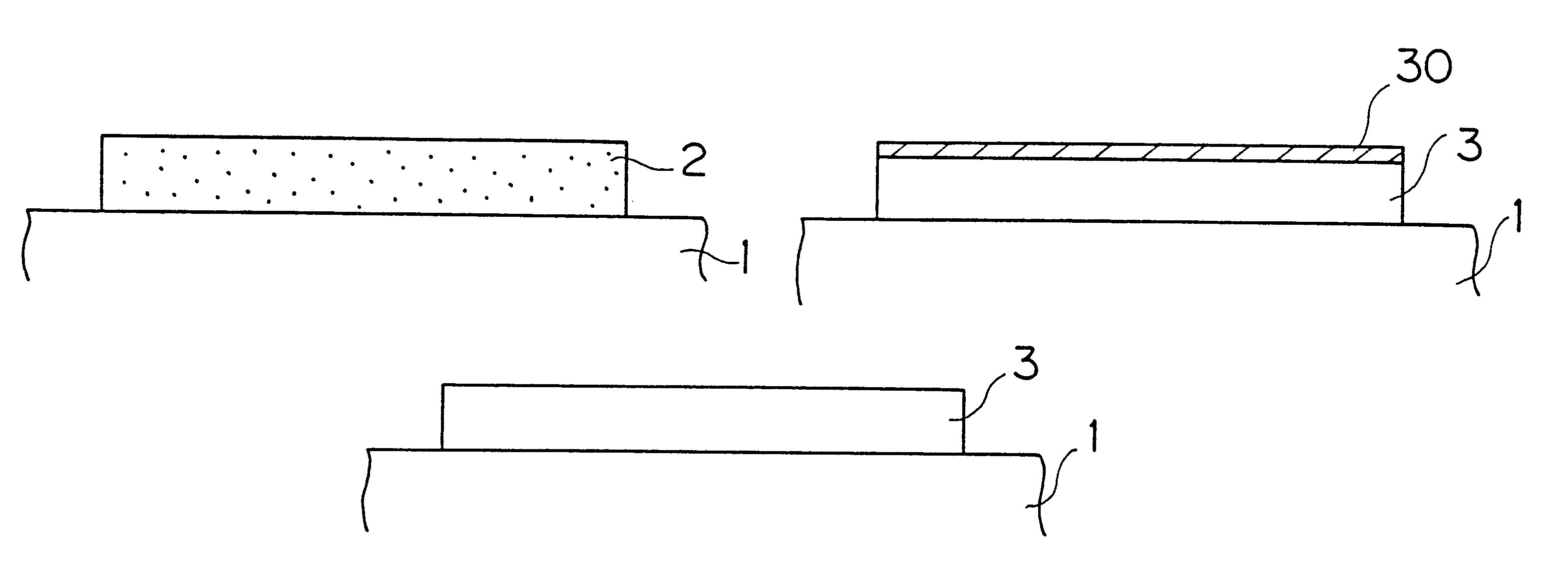
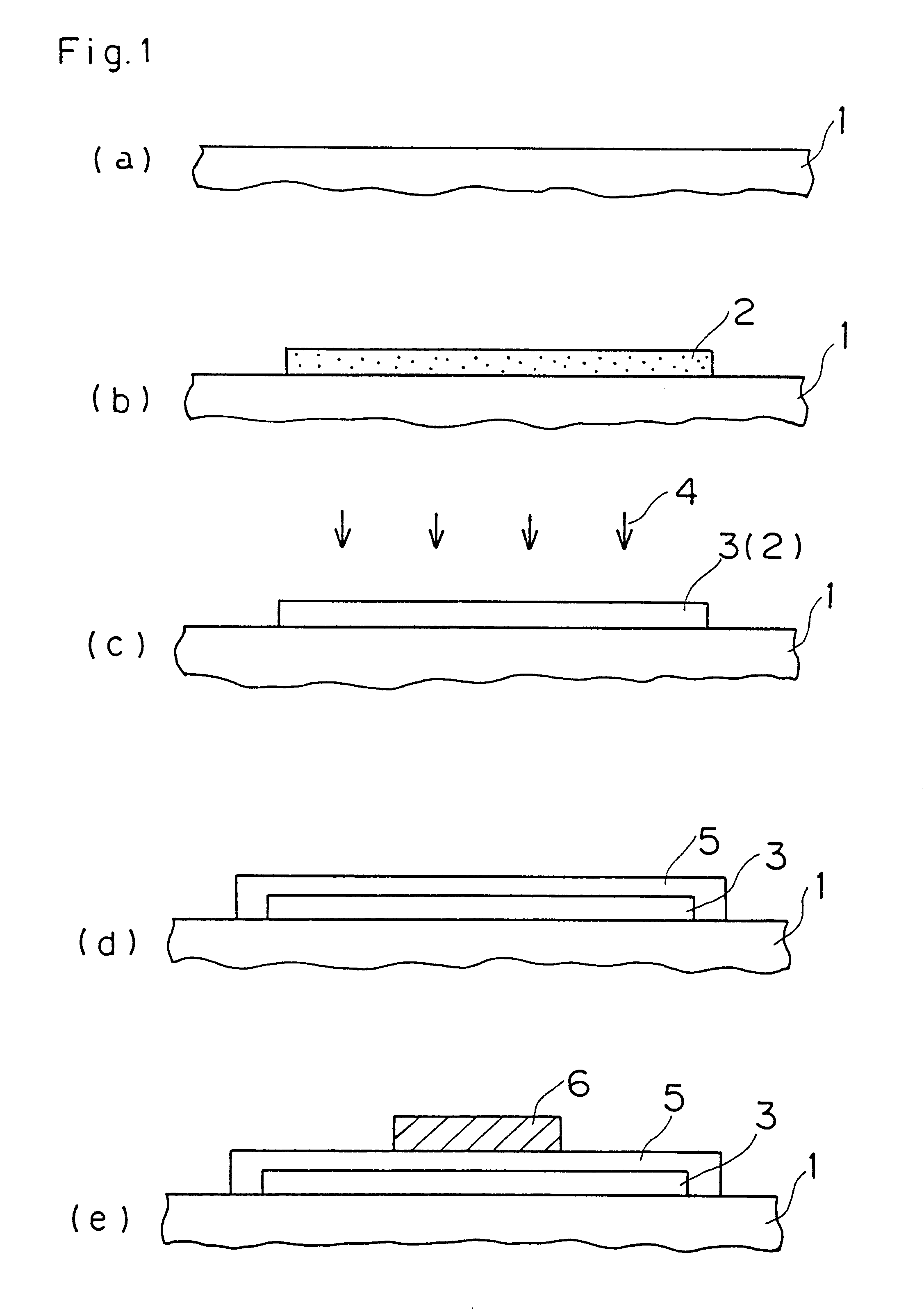
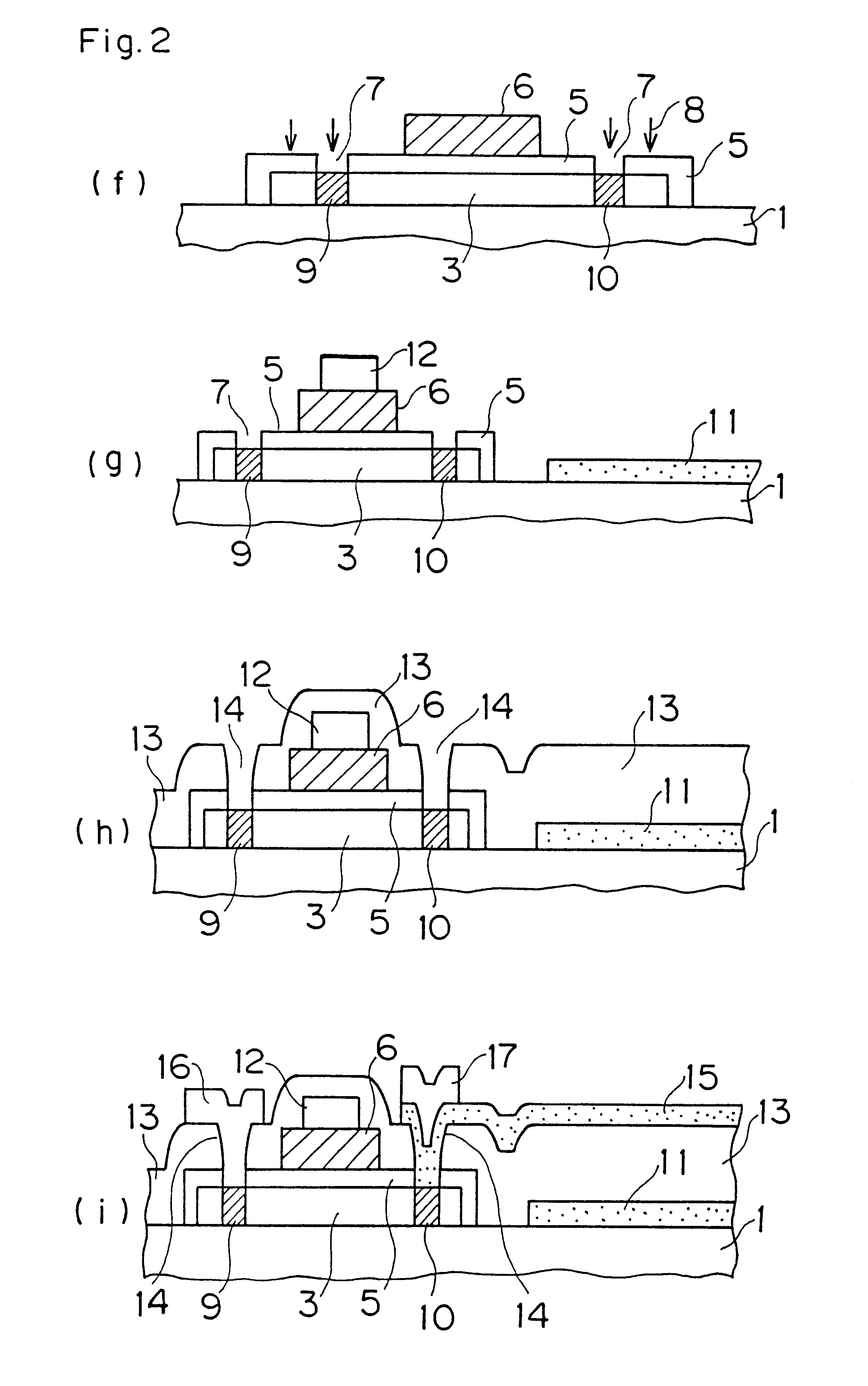
While the removal of oxygen which is an impurity in the film and the solid-phase epitaxy of the amorphous silicon film are simultaneously carried out by a single heat treatment in the aforementioned method according to the second embodiment, these steps may alternatively be carried out independently of each other. FIGS. 13(a) to 13(d) are explanatory diagrams showing steps of fabricating a polycrystalline silicon film by such a method.

The steps shown in FIGS. 13(a) and 13(b) are similar to those of the second embodiment described with reference to FIGS. 9(a) and 9(b), and hence redundant description is omitted.

Following these steps, a heat treatment is performed at a low temperature causing no crystallization of an amorphous silicon film 2 to be capable of removing oxygen from the film in this embodiment, as shown in FIG. 13(c). In this case, heat treatment conditions are set as follows:

First...

fourth embodiment

A fourth embodiment according to the second aspect of the present invention is now described.

FIGS. 15(a) to 15(d) are sectional views showing steps of fabricating a solar cell (photovoltaic device) according to the fourth embodiment of the present invention. The fabrication process for a polycrystalline silicon film according to the second aspect of the present invention is also applicable to a polycrystalline silicon electrode for a solar cell, as hereafter described. The steps of fabricating a solar cell are now described with reference to FIGS. 15(a) to 15(d).

First, an n-type amorphous silicon film 51 which is doped with phosphorus (P) and a non-doped amorphous silicon film 52 are continuously formed on a surface of a substrate 50 consisting of a high melting point metal by plasma CVD or the like, as shown in FIG. 15(a).

Then, a heat treatment is performed in a wet oxygen atmosphere, to epitaxially grow the n-type amorphous silicon film 51 and the non-doped amorphous silicon film ...


PUM


Abstract

A method of fabricating a semiconductor device includes the steps of forming an amorphous semiconductor film on a substrate, oxidizing the surface of the amorphous semiconductor film in an atmosphere containing water vapor and oxygen, and removing the oxide film which is formed on the surface of the semiconductor film.

Description

1. Field of the InventionThe present invention relates to a method of treating a semiconductor film and a method of fabricating a semiconductor device, and more particularly, it relates to a method of treating a semiconductor film of amorphous silicon or the like which can reduce impurity concentration and a method of fabricating a semiconductor device with the semiconductor film.2. Description of the Background ArtIn recent years, a semiconductor device employing a semiconductor layer of polycrystalline silicon which is much higher in carrier mobility than amorphous silicon has attracted much attention. Such a semiconductor device includes a thin film transistor (TFT).A conventional method of fabricating a thin film transistor employing the so-called solid-phase epitaxy of obtaining a polycrystalline silicon film by epitaxially growing an amorphous silicon film in a solid phase. FIGS. 17(a) to 17(e) and 18(f) to 18(i) illustrate steps of fabricating a thin film transistor which is ...

Claims


Application Information

Patent Timeline
IPC IPC(8): C30B1/02C30B33/00C30B1/00H01L21/20H01L21/02H01L27/146H01L21/316H01L21/324H01L21/336H01L27/10H01L27/12H01L29/78H01L29/786H01L31/04
CPCC30B1/023C30B33/005H01L21/2022C30B29/06H01L21/02667H01L21/02422H01L21/02488H01L21/02502H01L21/02395H01L21/0242H01L21/0262H01L21/02425H01L21/02686H01L21/02532H01L21/0245H01L21/02381
Inventor HAMADA, HIROKIHIRANO, KIICHISASAKI, AKIFUMI
Owner SANYO ELECTRIC CO LTD
Why Eureka
Try Eureka