Solid-state imaging device

a solid-state imaging and imaging pixel technology, applied in the field of solid-state imaging devices, can solve the problems of wasting a lot of light, wasting a lot of af processing time,

Inactive Publication Date: 2011-09-15
FUJIFILM CORP
View PDF7 Cites 48 Cited by
  • Summary
  • Abstract
  • Description
  • Claims
  • Application Information

AI Technical Summary

Benefits of technology

[0019]It is preferable that on a lens forming surface where each microlens is formed, a concave section is formed at a position corresponding to the dedicated imaging pixel arranged around the phase difference detection pixel, and that by forming the microlens on an inner bottom surface of the concave section, the height of the microlens arranged around the phase difference detection pixel from the photoelectric conversion element becomes lower than the height of the microlens of the phase difference detection pixel.
[0020]It is more preferable that by forming plural concave sections of different depth in the lens forming surface, the height of the microlens of the dedicated imaging pixel becomes lower progressively as its position becomes closer to the phase difference detection pixel.
[0022]It is preferable that on a lens forming surface where each microlens is formed, a convex section is formed at a position corresponding to the phase difference detection pixel, and that by forming the microlens on the convex section, the height of the microlens of the phase difference detection pixel becomes higher than the height of the microlens of the dedicated imaging pixel.
[0030]According to the present invention, the microlens of the dedicated imaging pixel arranged around the phase difference detection pixel is formed to be smaller than the microlens of the other dedicated imaging pixel. In this way, in the dedicated imaging pixel around the phase difference detection pixel, quantity of the light to be incident on the photoelectric conversion element from the microlens becomes lower. Therefore, since a size of the microlens is regulated so that light quantity from the microlens is lowered according to quantity of light to be incident from the gap between the microlens of the dedicated imaging pixel and the microlens of the phase difference detection pixel, light of approximately uniform light quantity can be incident on the photoelectric conversion element of each dedicated imaging pixel.

Problems solved by technology

However, since a focus lens needs to move to obtain a plurality of contrast evaluation values, the contrast detection method has a problem that it takes longer time for focusing in comparison with other methods.
However, in the configuration of Japanese Patent Laid-Open Publication No. 2004-361611, since the focus lens must move in the movement range although which can become narrower, speedup of the AF processing has a limit.
However, when the imaging surface is constituted of an arrangement of the phase difference detection pixels and the dedicated imaging pixels, it has a problem that a light receiving amount of the dedicated imaging pixel becomes high at a position adjacent to the phase difference detection pixel.
However, when the correction process is executed, additional time will be required for imaging.

Method used


Image

  • Solid-state imaging device
  • Solid-state imaging device
  • Solid-state imaging device

Examples


first embodiment

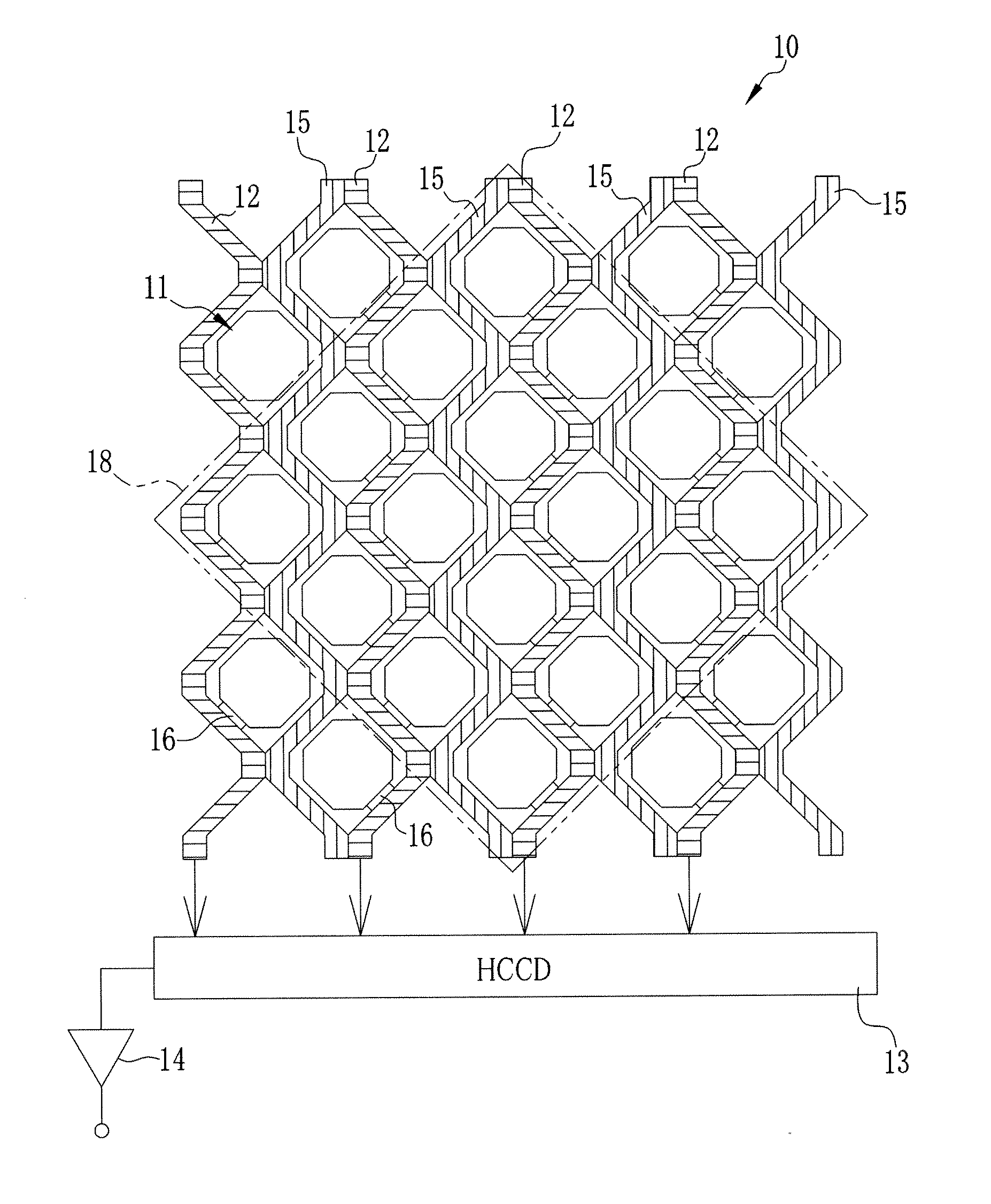
[0053]In FIG. 1, a CCD image sensor (solid-state imaging device) 10 includes a plurality of pixels 11, a plurality of vertical transfer paths (VCCD)12, a horizontal transfer path (HCCD) 13, and a floating diffusion amplifier (FDA) 14. The pixels 11 are arranged with a predetermined pitch in a vertical direction and a horizontal direction and accumulate electric charge depending on incident light. The VCCD 12 transfers the electric charge that each pixel 11 accumulated to the vertical direction. The HCCD 13 is connected to the end of each VCCD 12, and transfers the electric charge transferred from each VCCD 12 in the horizontal direction. The FDA 14 converts the electric charge transferred from the HCCD 13 into a voltage signal (an imaging signal) and outputs it. Between the adjacent pixels 11, there is a device isolation area 15 which electrically separates each pixel 11 so that the electric charge does not transferred.

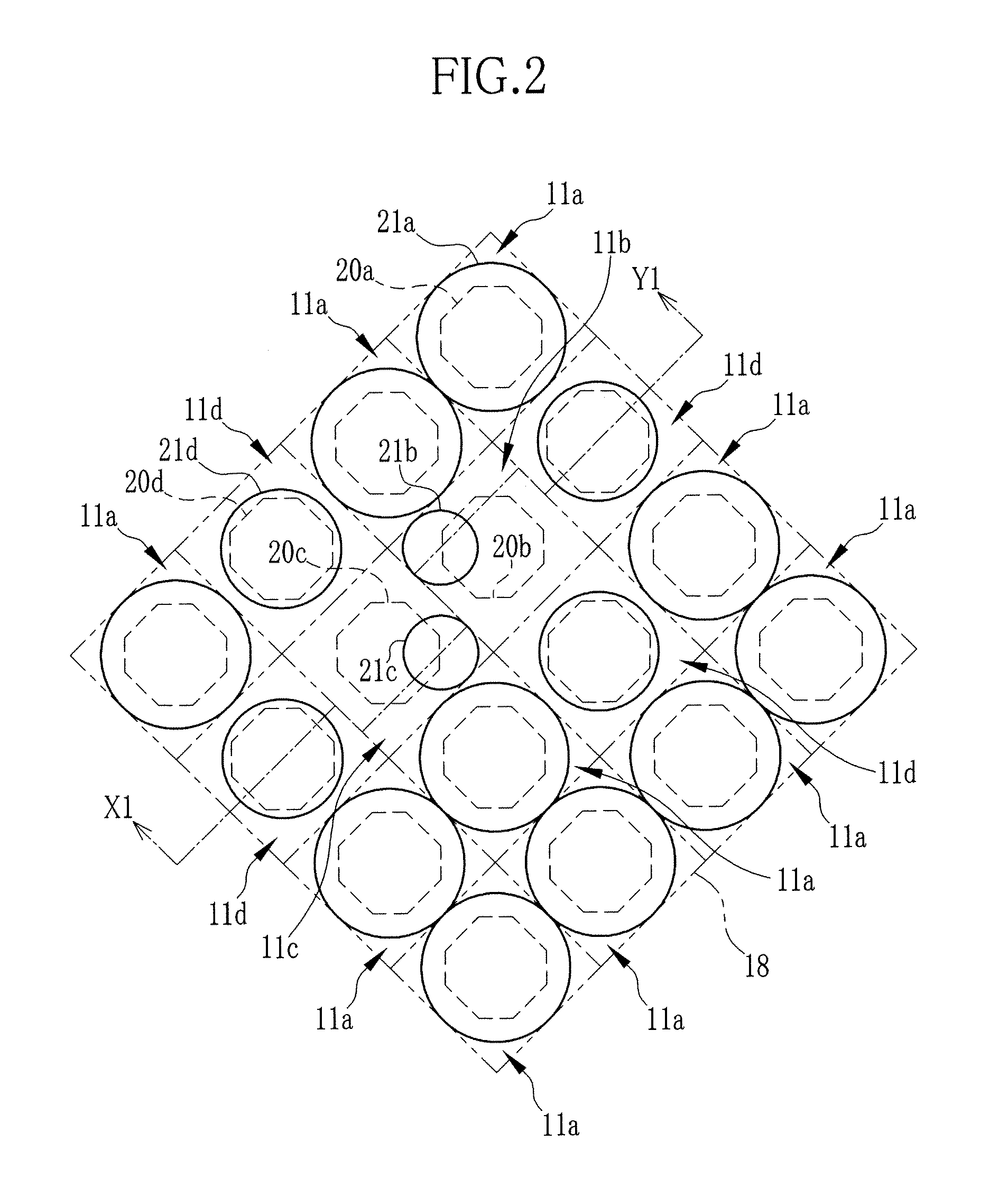
[0054]The pixels 11 have an arrangement in which that a tetragon...

second embodiment

[0078]Next, a second embodiment of the present invention will be explained. Note that it refers same reference numbers about the same components in functions and constitutions as the first embodiment described above, and omits detailed explanation of them. In the first embodiment described above, the pixel group 18 is composed of the four kinds of pixels which are the first pixel 11a to the fourth pixel 11d. In contrast, in this embodiment, as illustrated in FIG. 4, a pixel group 50 is composed of five kinds of pixels including a fifth pixel 11e in addition to the first pixel 11a to the fourth pixel 11d. The pixel group 50 is a replacement of the seven first pixels 11a adjacent to the fourth pixel 11d, among the ten first pixels 11a included in the pixel group 18 of the first embodiment, by the fifth pixels 11e.

[0079]The fifth pixel 11e is used for imaging forming at the time of execution of image capturing, with the first pixel 11a and the fourth pixel 11d. The fifth pixel 11e inc...

third embodiment

[0084]Next, a third embodiment of the present invention will be explained. In FIG. 5, like the pixel group 50 of the second embodiment described above, a pixel group 52 of this embodiment is comprised of the five kinds of pixels which are the first pixel 11a to the fifth pixel 11e. Of these, the first pixel 11a, the fourth pixel 11d, and the fifth pixel 11e which are the dedicated imaging pixel have the same constructions with those of the second embodiment.

[0085]On the other hand, the second pixel 11b has a microlens 53 having a diameter larger than the microlens 21b of the first and second embodiments. The microlens 53 is formed so that a part of it gets into a vacant space of the adjacent third pixel 11c and a vacant space of the adjacent fifth pixel 11e. Note that the vacant space is the space where the microlens is not formed on the lens forming surface 34a of the pixel.

[0086]Similarly, the third pixel 11c has a microlens 54 having a diameter larger than that of the microlens 2...


PUM


Abstract

A CCD image sensor which is a solid-state imaging device has four kinds of pixels of first pixel to fourth pixel arranged in a predetermined pattern. The each pixel has each PD and each microlens. The first pixel and the fourth pixel are dedicated imaging pixels. The fourth pixel is placed adjacent to the second pixel and the third pixel which are pixels for phase difference detection, and its microlens is formed smaller than the microlens of the first pixel. Accordingly, since quantity of the light to be incident on the PD from the microlens is lowered corresponding to the incident light from the gap between the microlenses, light with approximately uniform quantity is incident on the each PD.

Description

BACKGROUND OF THE INVENTION[0001]1. Field of the Invention[0002]The present invention relates to a solid-state imaging device, which includes plural dedicated imaging pixels and plural phase difference detection pixels and performs automatic focusing of phase difference method based on an image obtained from the phase difference detection pixel.[0003]2. Description of the Related Arts[0004]Digital cameras, which comprise solid-state imaging device such as a CCD image sensor or a CMOS image sensor and produce a digital image, become widespread. Most of the digital cameras include an autofocus (AF) function to automatically regulate the focus of an imaging lens, and as the AF function, a contrast detection method is widely adopted. Since it is not necessary to additionally provide a dedicated sensor for measuring a distance to a subject or a solid-state imaging device for AF, the contrast detection method has an advantage that the AF function can be realized with relatively low cost.[...

Claims


Application Information

Patent Timeline
Patent Type & Authority Applications(United States)
IPC IPC(8): H04N5/335
CPCG02B3/0043G02B7/34G02B7/36G03B13/36H04N5/372H01L27/14627H01L27/14812H01L27/14843H01L27/14605H04N25/71
Inventor AWAZU, KOUHEI
Owner FUJIFILM CORP
Why Eureka
Try Eureka