

Enhancement of LED light extraction with in-situ surface roughening
a surface roughening and led light technology, applied in the direction of polycrystalline material growth, crystal growth process, chemically reactive gas, etc., can solve the problems of limited external quantum efficiency of gan based leds, impeded their practical fabrication, and unsatisfactory light extraction efficiency, so as to enhance light extraction and improve external quantum efficiency
- Summary
- Abstract
- Description
- Claims
- Application Information
AI Technical Summary
Benefits of technology
Problems solved by technology
Method used
Image

Examples
Embodiment Construction
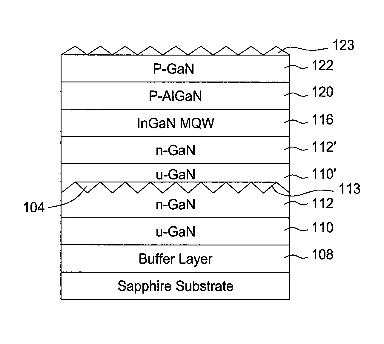
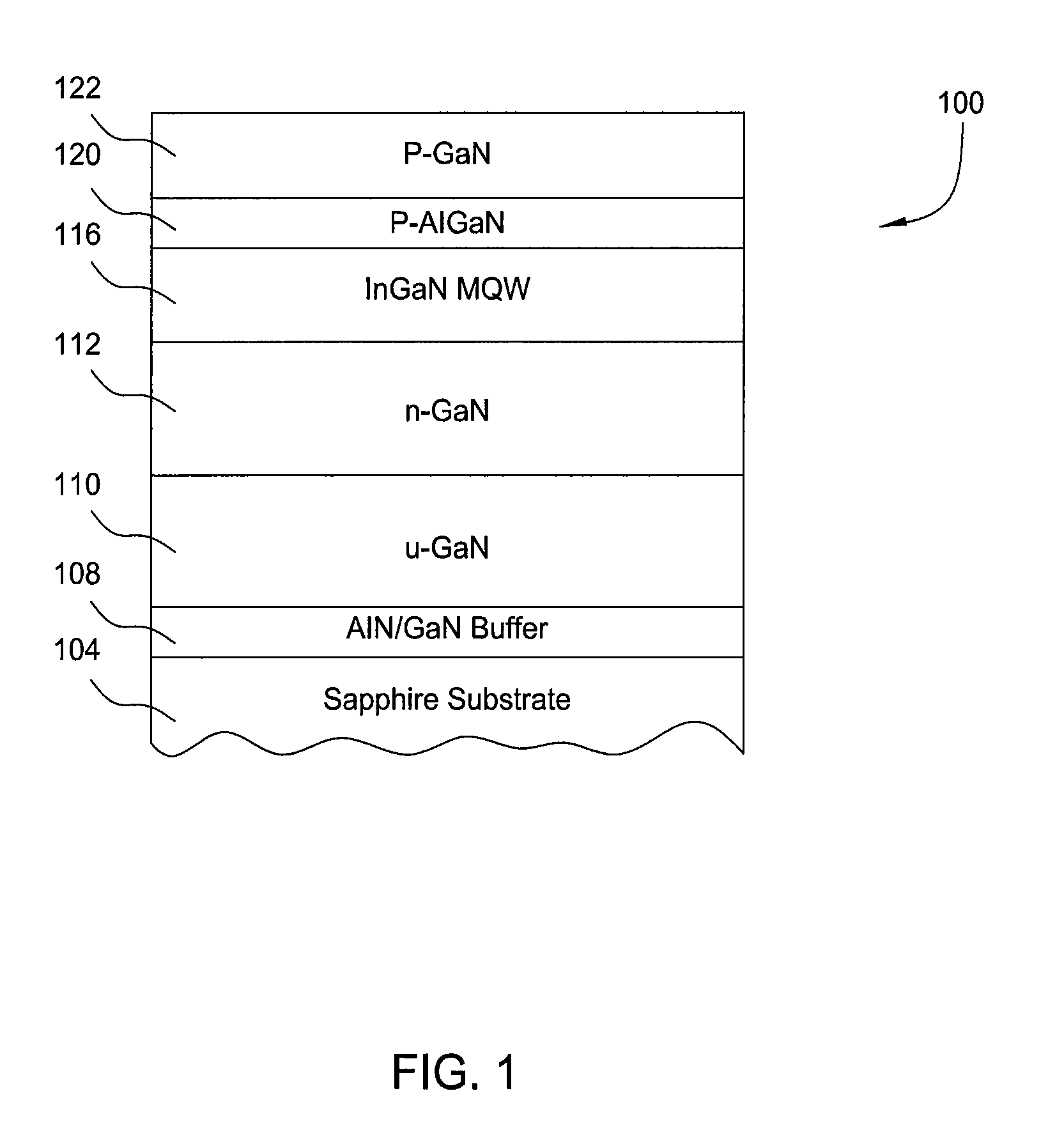
[0023]Embodiments described herein generally relate to methods for forming Group III-V materials used in optoelectronic devices, such as light emitting diodes (LEDs) and laser diodes (LDs). Particularly, embodiments of the present invention provide methods for enhancing the light extraction by surface roughening of the bottom n-GaN layer and / or top p-GaN so that the internal light from the active region is scattered outwardly to result in higher external quantum efficiency. In one embodiment, a surface roughening process is performed on an n-doped GaN (n-GaN) layer to form etching pits in a top surface of the n-GaN layer. Once the etching pits are formed, growth of the n-GaN material may be resumed on the roughened n-GaN layer to partially fill the underlying etching pits, thereby forming air voids or bubbles at the interface of the n-GaN layer and the subsequent, re-growth n-GaN layer. These voids or bubbles are believed to provide one or more localized regions with indices of refl...
PUM
| Property | Measurement | Unit |
|---|---|---|
| Nanoscale particle size | aaaaa | aaaaa |
| Nanoscale particle size | aaaaa | aaaaa |
| Surface roughness | aaaaa | aaaaa |
Abstract
Description
Claims
Application Information