Field-effect transistor

a field-effect transistor and transistor technology, applied in the field of field-effect transistors, can solve the problems of insufficient resistance, insufficient resistance, and insufficient resistance reduction, and achieve the effect of low resistance, low on-resistance and reduced contact resistance of source electrode and drain electrod

Inactive Publication Date: 2011-09-22
PANASONIC CORP
View PDF16 Cites 27 Cited by
  • Summary
  • Abstract
  • Description
  • Claims
  • Application Information

AI Technical Summary

Benefits of technology

[0032]According to this configuration, the contact resistance of the source electrode and the drain electrode can be reduced.
[0033]According to the present invention, low on-resistance can be realized in a FET made of nitride semiconductors.

Problems solved by technology

However, with the conventional FETs using a group-III nitride semiconductor, on-resistance is not sufficiently low and further reduction of on-resistance is required.
Furthermore, in a normally-off FET, the gate-source parasitic resistance and gate-drain parasitic resistance have a tendency to increase, and, although the FET in Patent Reference 1 takes into account the increase in parasitic resistance by suppressing the effects of surface levels, further reduction in resistance is required.

Method used


Image

  • Field-effect transistor
  • Field-effect transistor
  • Field-effect transistor

Examples


embodiment 1

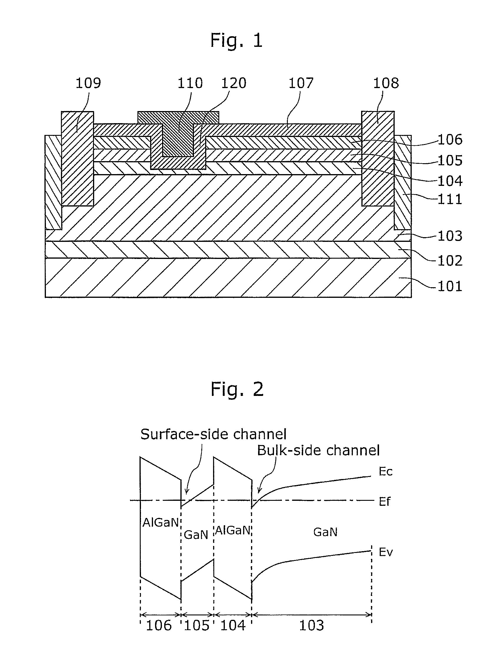
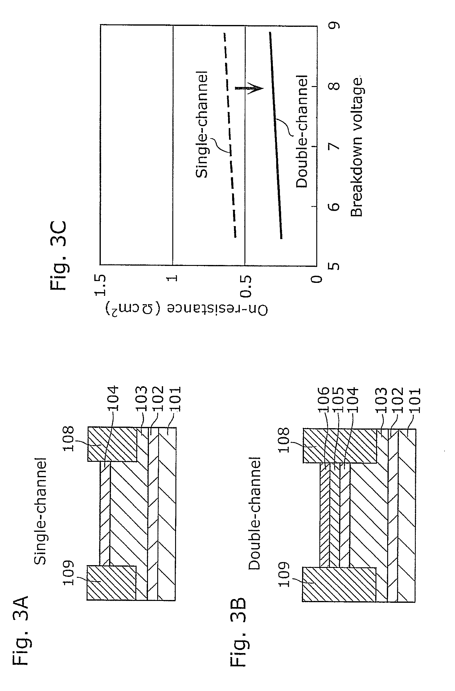
[0048]Hereinafter, a configuration of a FET in Embodiment 1 of the present invention and a manufacturing method thereof shall be described.

[0049]FIG. 1 is a cross-sectional view of a configuration of a display device according to the present embodiment.

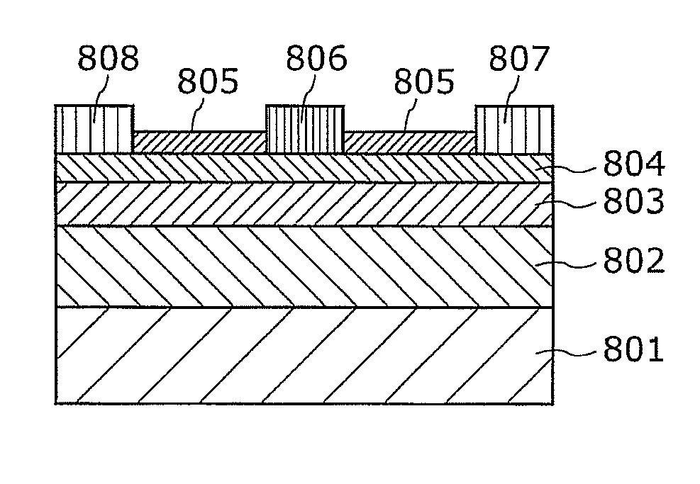
[0050]The FET includes a substrate 101, a buffer layer 102, a first nitride semiconductor layer 103, a second nitride semiconductor layer 104, a third nitride semiconductor layer 105, a fourth nitride semiconductor layer 106, an insulating film 107, a drain electrode 108, a source electrode 109, a gate electrode 110, and an element separation layer 111.

[0051]The substrate 101 is, for example, a sapphire substrate, a SiC substrate, a Si substrate, a GaN substrate, and so on, having a thickness (film-thickness) of between 10 μm to 1000 μm, inclusive.

[0052]The buffer layer 102 is made of AlN having a thickness, for example, 100 nm, that depends on the substrate 101, and is formed on the substrate 101.

[0053]The first nitride semiconductor...

embodiment 2

[0077]Hereinafter, a configuration of a FET in Embodiment 2 of the present invention and a manufacturing method thereof shall be described.

[0078]FIG. 4 is a cross-sectional view of a configuration of the FET according to the present embodiment.

[0079]The FET includes a substrate 201, a buffer layer 202, a first nitride semiconductor layer 203, a second nitride semiconductor layer 204, a third nitride semiconductor layer 205, a fourth nitride semiconductor layer 206, an insulating film 207, a drain electrode 208, a source electrode 209, a gate electrode 210, and an element separation layer 211.

[0080]The substrate 201 is, for example, a sapphire substrate, a SiC substrate, a Si substrate, a GaN substrate, and so on, having a thickness of between 10 μm to 1000 μm, inclusive.

[0081]The buffer layer 202 is made of AlN having a thickness, for example, 100 nm, that depends on the substrate 201, and is formed on the substrate 201.

[0082]The first nitride semiconductor layer 203 is made of, for...

embodiment 3

[0103]Hereinafter, a configuration of a FET in Embodiment 3 of the present invention and a manufacturing method thereof shall be described.

[0104]FIG. 5 is a cross-sectional view of a configuration of the FET according to the present embodiment.

[0105]The FET includes a substrate 301, a buffer layer 302, a first nitride semiconductor layer 303, a second nitride semiconductor layer 304, a third nitride semiconductor layer 305, a fourth nitride semiconductor layer 306, an insulating film 307, a drain electrode 308, a source electrode 309, a gate electrode 310, an element separation layer 311, and a fifth nitride semiconductor layer 312.

[0106]The substrate 301 is, for example, a sapphire substrate, a SiC substrate, a Si substrate, a GaN substrate, and so on, having a thickness of between 10 μm to 1000 μm, inclusive.

[0107]The buffer layer 302 is made of AlN having a thickness, for example, 100 nm, that depends on the substrate 301, and is formed on the substrate 301.

[0108]The first nitrid...


PUM

PropertyMeasurementUnit
thicknessaaaaaaaaaa
thicknessaaaaaaaaaa
thicknessaaaaaaaaaa

Abstract

The present invention has as an object to provide a FET having low on-resistance. The FET according to the present invention includes: first nitride semiconductor layer; a second nitride semiconductor layer formed on the first nitride semiconductor layer and having a higher band gap energy than the first nitride semiconductor layer; a third nitride semiconductor layer formed on the second nitride semiconductor layer; a fourth nitride semiconductor layer formed on the third nitride semiconductor layer and having a higher band gap energy than the third nitride semiconductor layer. A channel is formed in a heterojunction interface between the first nitride semiconductor layer and the second nitride semiconductor layer.

Description

CROSS REFERENCE TO RELATED APPLICATION[0001]This is a continuation application of PCT application No. PCT / JP2009 / 006038 filed on Nov. 12, 2009, designating the United States of America.BACKGROUND OF THE INVENTION[0002](1) Field of the Invention[0003]The present invention relates to field-effect transistors, and particularly relates to a field-effect transistor made of a group-III nitride semiconductor.[0004](2) Description of the Related Art[0005]Group-III nitride semiconductors represented by gallium nitride (GaN) semiconductors have a wide band gap, high breakdown field, and high saturated electron velocity which exceed those of semiconductors made of silicon or gallium arsenide. Due to this physical advantage, field-effect transistors (FETs) using a group-III nitride semiconductor show much potential as next-generation radio frequency devices or high-power switching devices, and are thus the subject of widespread research and development.[0006]Although the aforementioned FETs are...

Claims


Application Information

Patent Timeline
Patent Type & Authority Applications(United States)
IPC IPC(8): H01L29/205
CPCH01L29/2003H01L29/4236H01L29/7787H01L29/42316
Inventor ANDA, YOSHIHARUISHIDA, HIDETOSHIUEDA, TETSUZO
Owner PANASONIC CORP
Why Eureka
Try Eureka