Semiconductor device and semiconductor device manufacturing method

a semiconductor device and manufacturing method technology, applied in the direction of semiconductor devices, circuit arrangements on conductive chasis, basic electric elements, etc., can solve the problems of mutual interaction between the inductor elements, poor inductor element performance, circuit malfunction, etc., to reduce the design of the semiconductor device containing the inductor element, reduce the design freedom, and effectively suppress the mutual interaction

Active Publication Date: 2011-09-29
RENESAS ELECTRONICS CORP
View PDF19 Cites 15 Cited by
  • Summary
  • Abstract
  • Description
  • Claims
  • Application Information

AI Technical Summary

Benefits of technology

[0018]The inventors perceived the fact that in semiconductor devices utilizing numerous inductor elements such as in high-speed logic circuits allowing a comparatively low Q value compared to wireless circuits, the effect that the wiring exerts in inductor elements can be suppressed by installing a shielded conductor at a fixed voltage potential between the inductor element and the wiring positioned above the inductor element in semiconductor devices containing inductor elements utilizing lower layer wiring layers.
[0019]The present invention can in other words achieve a semiconductor device that occupies a minimal area because the designer can freely install an external coupled pad or wiring at a fixed voltage potential above an inductor element utilized in high-speed logic circuits. The man-hours required for designing the semiconductor device containing the inductor element can also be reduced since there is greater design freedom by placement above the inductor element.
[0020]The present invention is therefore capable of effectively suppressing the mutual interaction that occurs between the inductor element and the wiring positioned above the inductor element in the same chip.

Problems solved by technology

When inductor elements are mounted overlying a semiconductor substrate, eddy current loss due to magnetic fields penetrating to the semiconductor substrate positioned below the inductor element, and wiring near the inductor element cause poor inductor element performance.
The circuit design therefore positions the wiring above the inductor elements causing the problem of mutual interaction between the inductor element and the wiring.
A mutual interaction consequently occurs between the inductor elements and the wiring that causes poor inductor element characteristics due to losses in wires at a fixed voltage potential and leads to circuit malfunctions.
However this method not only led to a loss of freedom in wiring circuit design but also led to utilizing a greater area of the chip.
Moreover, forming a pad overlying the inductor element for making external couplings was impossible and therefore also led to a large increase in the chip area of the semiconductor device.

Method used


Image

  • Semiconductor device and semiconductor device manufacturing method
  • Semiconductor device and semiconductor device manufacturing method
  • Semiconductor device and semiconductor device manufacturing method

Examples


first embodiment

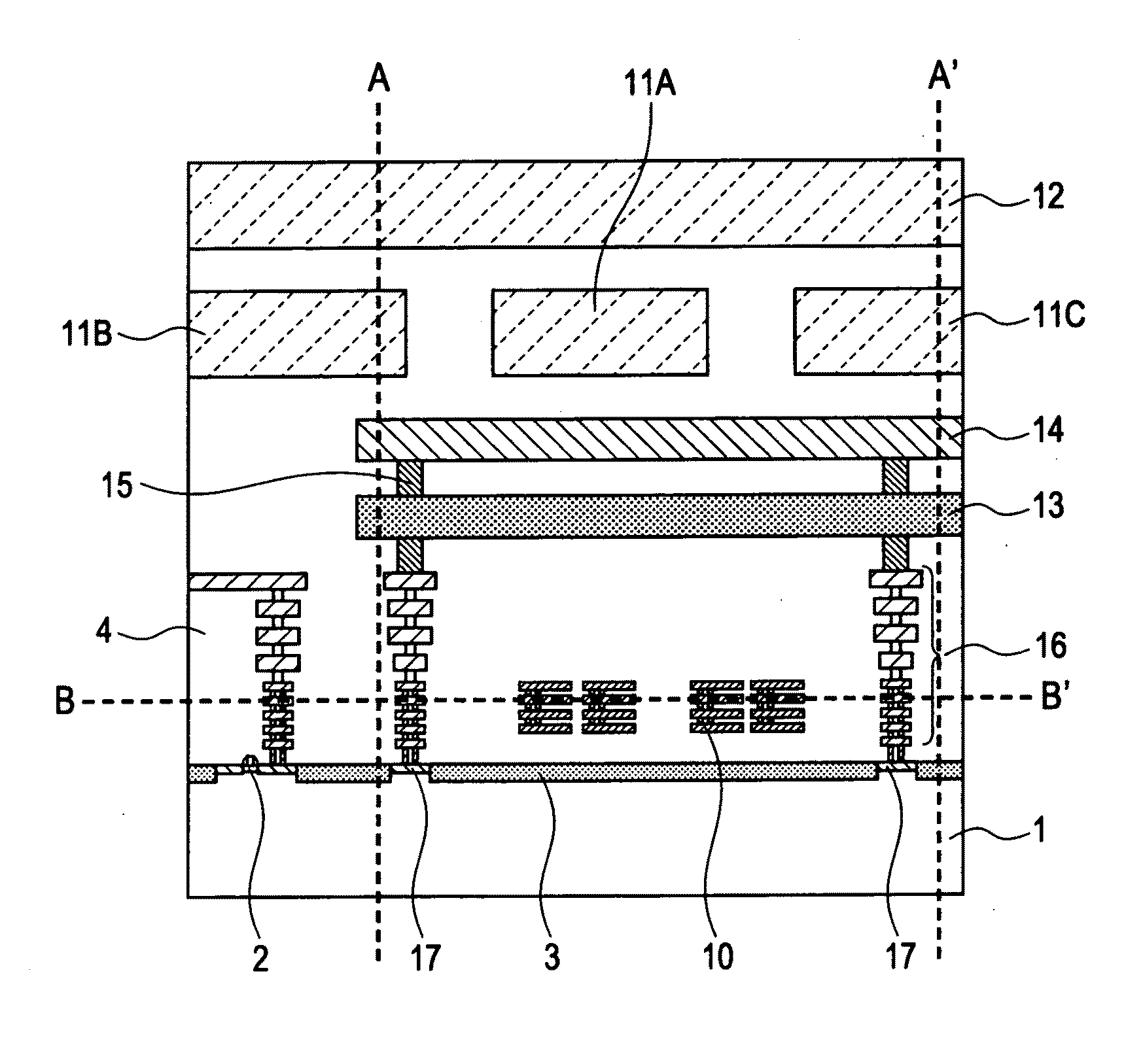
[0049]FIG. 1 is a cross sectional view showing one diagrammatic example of the first embodiment. Examining FIG. 1 reveals that an active element 2, an element isolation region 3, and an interlayer dielectric film 4 are formed over a semiconductor substrate 1 the same as a typical semiconductor device; and multiple wiring layers are also formed within the interlayer dielectric film 4. The semiconductor device of the present embodiment in other words includes the semiconductor substrate 1, and multiple wiring layers (hereafter multi-wiring layers) formed over the semiconductor substrate 1. These multi-wiring layers contain an inductor element 10, the wires 11A through 11C, and the wires 12 formed above the inductor element 10, and the shielded conductors 13 and 14 at a fixed voltage potential and formed between the inductor element and the wires 11A through 11C and the wires 12 so as to cover the inductor element 10 as seen from a flat view. The “wires 11A through 11C” are sometimes h...

second embodiment

[0089]The second embodiment of the present invention is described next in detail while referring to the drawings.

[0090]FIG. 12 is a cross sectional view showing one example of this embodiment. The second embodiment is different from the first embodiment in the shielded conductor 21 positioned between the inductor element 10, and the wires 11 and 12 positioned above the inductor element 10 is single layer wiring. However aside from this point, the second embodiment is identical to the first embodiment so a description is omitted here as appropriate for purposes of simplicity.

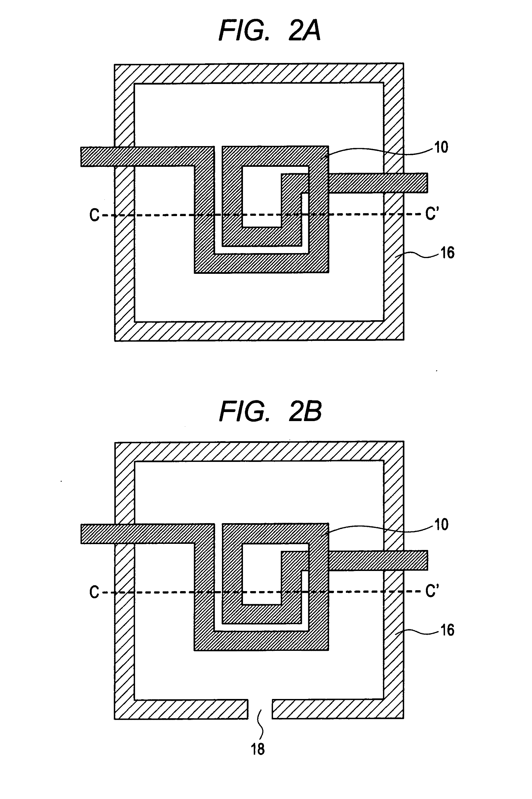
[0091]The shielded conductor 21 is a pattern in which a slit is formed the same as in the shielded conductor 14 in the first embodiment. Multiple wires are formed in the slit, and the wiring may be formed at a right angle to the electrical current flowing in the inductor element 10 directly below the direction the wire extends (See FIG. 3). The shielded conductor 21 may be formed in a matrix pattern to enhance th...

third embodiment

[0098]The third embodiment of the present invention is described next in detail while referring to the drawings.

[0099]FIG. 14 is a cross sectional view showing one example of the embodiment. Among the shielded conductors formed from two-layer wiring in the example shown in FIG. 14, the shielded conductor 13 positioned in the lower layer is a shielded conductor formed as shown in FIG. 3 the same as in the first embodiment; and the shielded conductor 22 positioned in the upper layer is a shielded conductor containing a matrix pattern as shown in FIG. 15. Namely, unlike the first embodiment, the present embodiment contains at least one each of a “shielded conductor containing a matrix pattern” and a “shielded conductor” that includes shielded conductor wires electrically coupled to each other, and the direction that the wiring positioned in the area overlapping the inductor element 10 extends as seen from a flat view is approximately perpendicular to the flow of electrical current in t...


PUM


Abstract

A semiconductor device and manufacturing method to effectively suppress the problem of mutual interaction occurring between an inductor element and wires positioned above the inductor element formed over the same chip. A semiconductor device includes a semiconductor substrate and a multi-wiring layer formed overlying that semiconductor substrate, and in which the multi-wiring layer includes: the inductor element and three successive wires and a fourth wire formed above the inductor element; and two shielded conductors at a fixed voltage potential and covering the inductor element as seen from a flat view, and formed between the inductor element and three successive wires and a fourth wire formed above the inductor element.

Description

CROSS-REFERENCE TO RELATED APPLICATIONS[0001]The disclosure of Japanese Patent Application No. 2010-67383 filed on Mar. 24, 2010 including the specifications, drawings and abstract is incorporated herein by reference in its entirety.BACKGROUND[0002]1. Field of the Invention[0003]The present invention relates to a semiconductor device and to a manufacturing method for a semiconductor device.[0004]2. Description of Related Art[0005]Increased performance of semiconductor devices in recent years has resulted in practical semiconductor devices operating at high frequencies exceeding the gigahertz level. This improved performance is mostly due to greater miniaturization of circuit elements mainly achieved by tinier gate lengths and suppressing short channel effects to reach higher operating frequencies. In semiconductor devices using signals in the high frequency bands at the gigahertz level or higher, inductor elements must often be highly integrated onto the semiconductor substrate to a...

Claims


Application Information

Patent Timeline
Patent Type & Authority Applications(United States)
IPC IPC(8): H05K7/02
CPCH01L23/5225H01L23/5227H01L2924/0002H01L2924/00
Inventor HIJIOKA, KENICHIROTANABE, AKIRAHAYASHI, YOSHIHIRO
Owner RENESAS ELECTRONICS CORP
Why Eureka
Try Eureka