Integrated circuit 3D memory array and manufacturing method
- Summary
- Abstract
- Description
- Claims
- Application Information
AI Technical Summary
Benefits of technology
Problems solved by technology
Method used
Image

Examples
Embodiment Construction
[0024]A detailed description of embodiments of the present invention is provided with reference to the FIGS. 1-16.
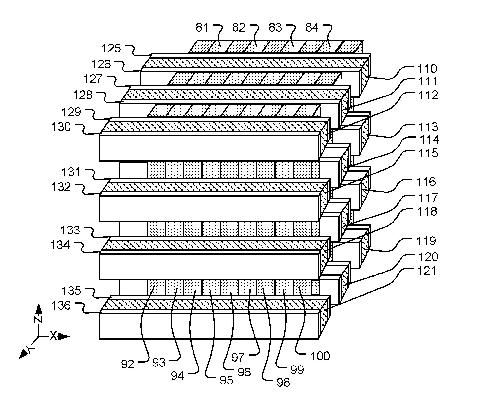
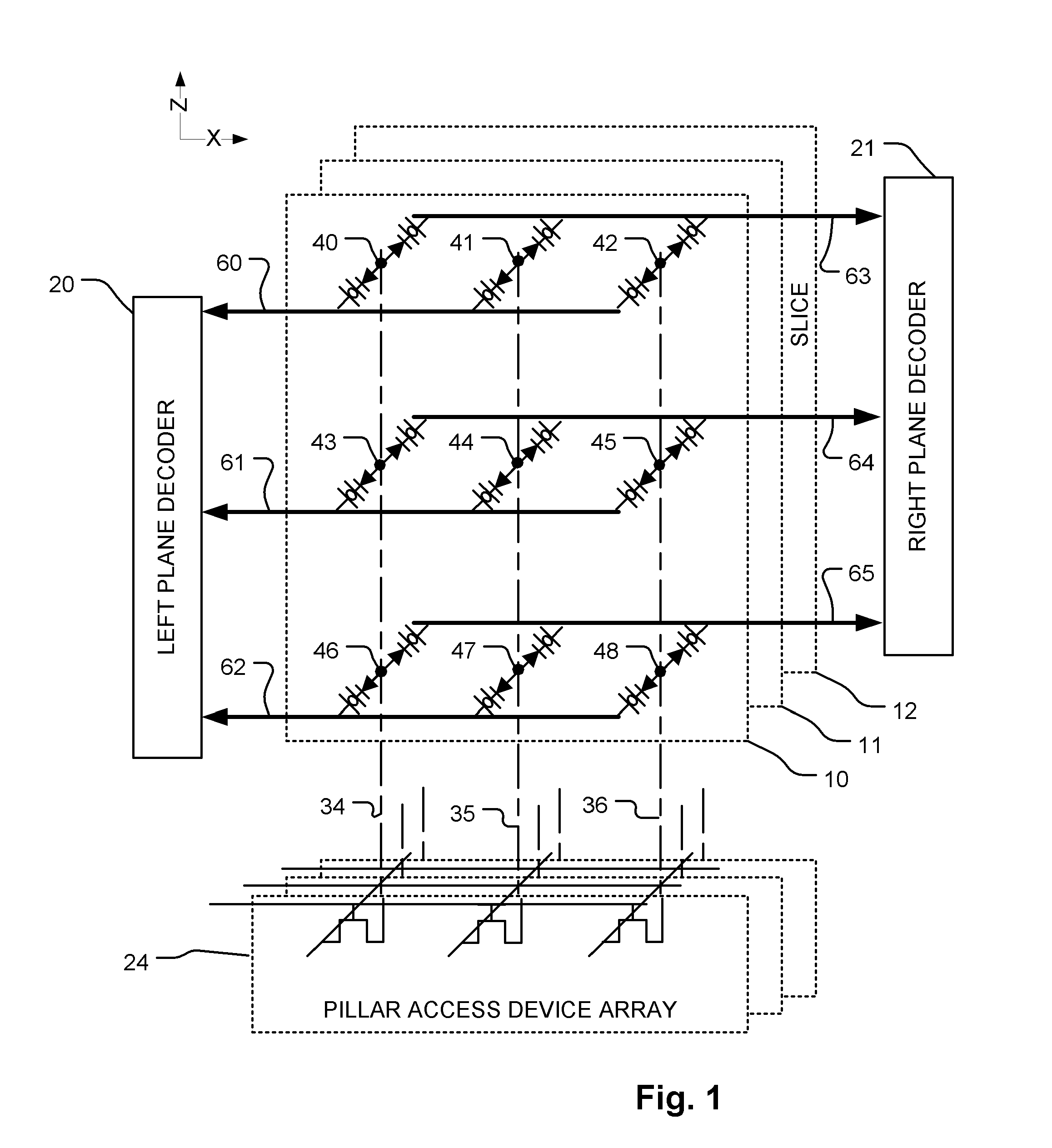
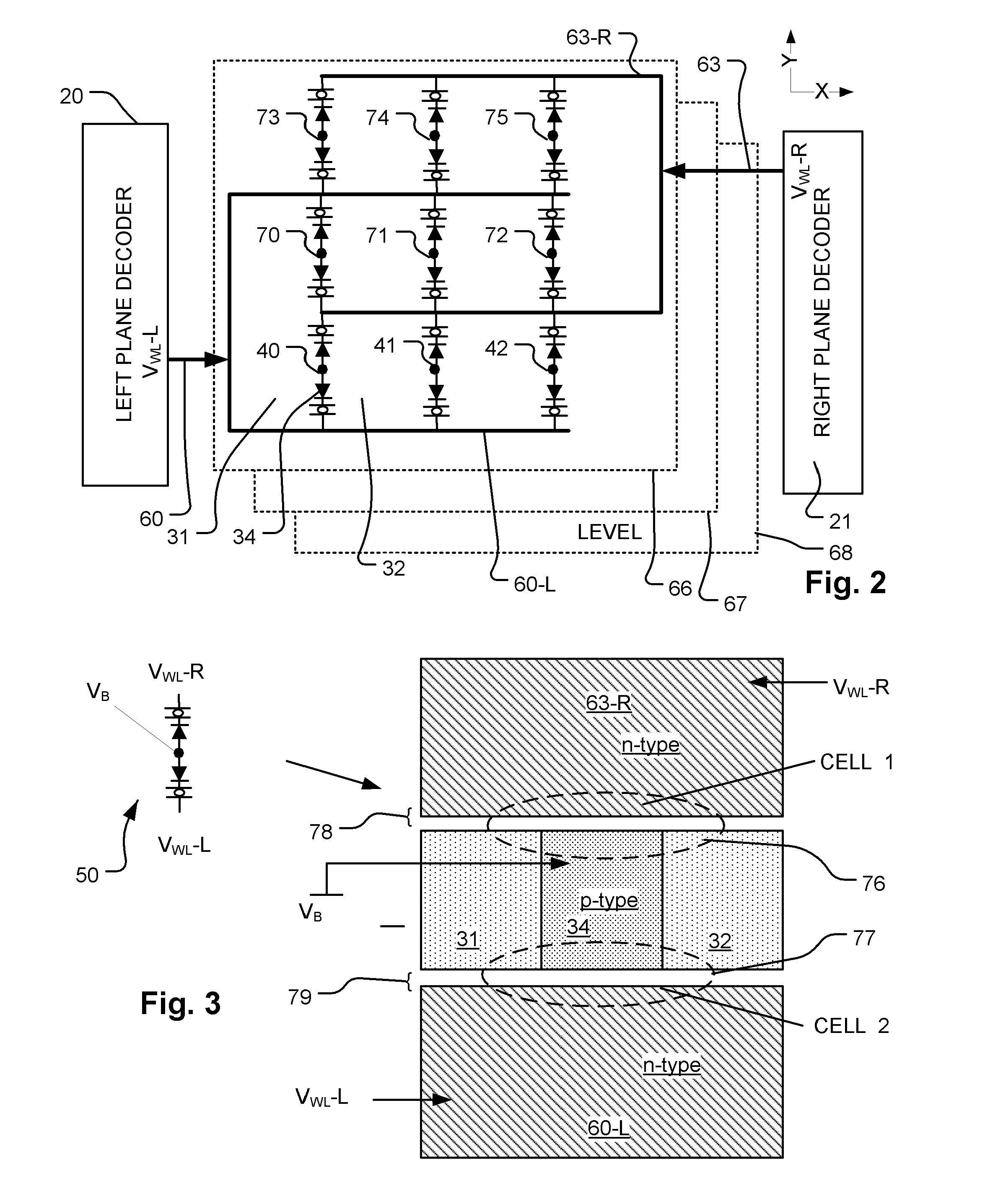
[0025]FIG. 1 is a schematic diagram of a 3D memory device, showing “slices”10, 11, 12 which lie in X-Z planes of the 3D structure. In the illustrated schematic, there are nine two-cell unit structures 40-48, each unit structure having two memory cells having separate programmable elements and left and right gates. Embodiments of the 3D memory device can include many two-cell unit structures per slice. The device includes an array of cells arranged for left and right decoding, using a left plane decoder 20, right plane decoder 21, and pillar access device array 24. The semiconductor pillars of the two-cell unit structures in a Z-direction column (e.g. 40, 43, 46) are coupled via a semiconductor pillar (e.g. 34) to an access device in a pillar access device array 24, implemented for example in the integrated circuit substrate beneath the structure. Likewise, the pillars fo...
PUM
 Abstract
Description
Claims
Application Information