
Display with in-cell touch sensor

a touch sensor and display technology, applied in the field of display, can solve the problems of degrading the transmittance of light and color rendering of the overall display and touch panel, the inability to integrate the etching process for the transparent substrate into the display manufacturing steps, and the inability to achieve the effect of reducing the display manufacturing cos

Active Publication Date: 2011-10-06
AROLLTECH
View PDF17 Cites 134 Cited by
  • Summary
  • Abstract
  • Description
  • Claims
  • Application Information

AI Technical Summary

Benefits of technology

[0007]The present invention provides a display integrated with a touch control unit, or a display with in-cell touch sensor. Some materials used in conventional touch panels are not required in the disclosed display. Therefore, some part of the touch control unit is implemented into conventional display manufacturing processes, effectively reducing the display manufacture cost.

Problems solved by technology

In addition, the assembly and alignment of such a display and a touch panel creates another issue.
Further, a plurality of photo etching processes are required to produce touch panel such that the etching processes for the transparent substrate cannot be integrated into the display manufacturing steps.
In addition, the transmittance of the light and color rendering of overall display and touch panel may degrade due to one additional separate touch sensor on top of the display.

Method used


Image

  • Display with in-cell touch sensor
  • Display with in-cell touch sensor
  • Display with in-cell touch sensor

Examples


Embodiment Construction

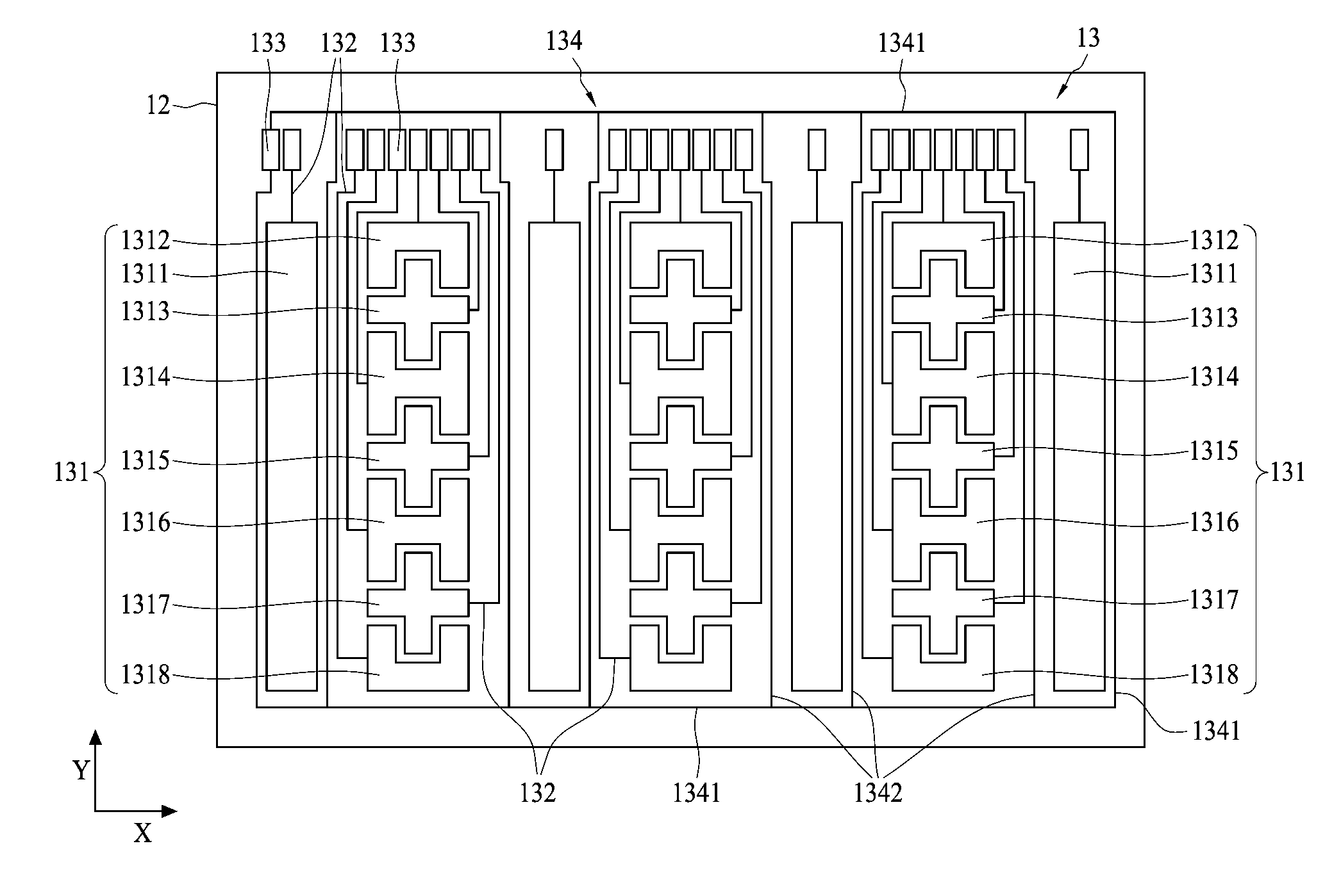
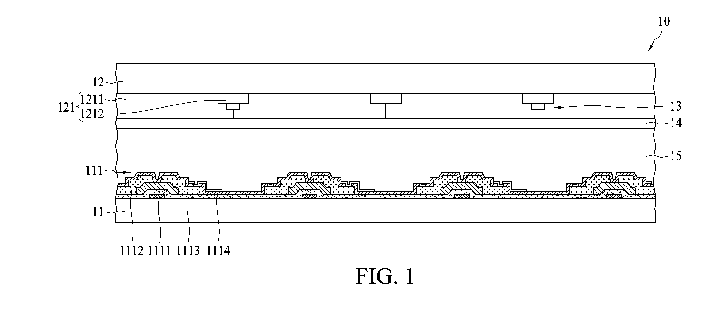
[0020]FIG. 1 shows a cross-sectional view of a display with in-cell touch panel apparatus according to an embodiment of the present invention. The display 10 comprises a first substrate 11, a second substrate 12 and a touch sensor 13 disposed on the surface of the second substrate 12. A thin-film transistor (TFT) array 111 is disposed on a surface of the first substrate 11. A color filter apparatus 121 comprising a color pixel array is disposed on a surface of the second substrate 12. A polarizer is disposed on the opposite surface of the second substrate 12 (not shown in the figure). However, the applications of the present invention are not just limited to LCD panel only, but can also be applied to self-emitting displays such as AMOLEDs or plasma displays. The active matrix thin-film transistor (TFT) can also be made by amorphous silicon (a-TFT), low-temperature poly-silicon (LTPS), organic TFT, or oxide TFT. The applications should cover any kinds of displays having active-matrix...


PUM


Abstract

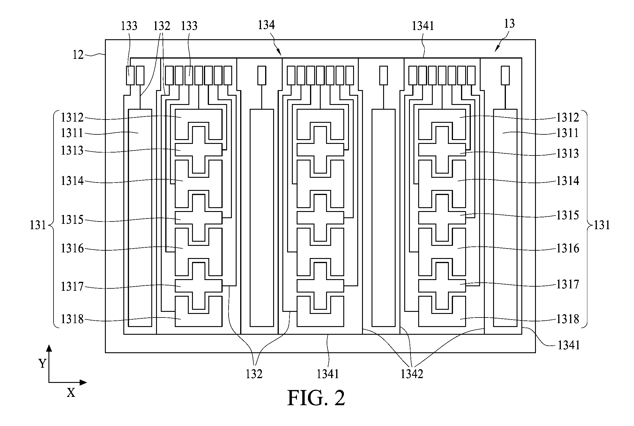
The present invention discloses a display with in-cell touch sensors comprising a first substrate, a second substrate, and a touch sensor disposed on the second substrate. A thin-film transistor (TFT) array is disposed on a surface of the first substrate, and a color pixel array is disposed on a surface of the second substrate. The TFT array faces and is aligned with the color pixel array. The touch sensor comprises a plurality of electrodes, a plurality of first leads, and a plurality of first pads. Each of the first leads is connected to one of the electrodes and one of the first pads. There are a plurality of second pads, a plurality of second leads, a plurality of connecting wires, and a plurality of terminal pads. Each of the second leads connects one of the second pads and one of the connecting wires. At least one of the connecting wires simultaneously and electrically connects several of the second leads. Each of the connecting wires electrically connects at least one of the terminal pads. Each of the first pads electrically connects one of the second pads.

Description

BACKGROUND OF THE INVENTION[0001]1. Field of the Invention[0002]The present invention relates to a display, and more particularly, to a display with in-cell touch sensor.[0003]2. Description of the Related Art[0004]Touch panels have been widely used in several fields such as house wares, ATM machines, communication apparatuses and electronic information devices. Among these fields, touch panels are mostly used as an input interface of TVs, smart phones, all-in-one PCs, notebooks, global positioning systems (GPS) and digital still cameras (DSC). That is, touch panels are mostly used as the media for selecting and operating displays, such as liquid crystal displays (LCD), active matrix organic light-emitting devices (AMOLED) and plasma displays. Currently, a touch panel can be integrated with a display such that a user can select representative icons shown on the selective panel by using a finger or a touch pen for the smart phones, GPS or DSC to execute a preferred function. This kin...

Claims


Application Information

Patent Timeline
IPC IPC(8): G06F3/041
CPCG06F3/047G06F3/0412G02F1/1333G02F1/13338
Inventor CHANG, YIH
Owner AROLLTECH
Learn More