Semiconductor device having transistor and rectifier

a technology of semiconductor devices and rectifiers, which is applied in the direction of semiconductor devices, basic electric elements, electrical appliances, etc., can solve the problems of difficult to achieve the reduction of forward voltage of the second diode without deterioration, and the former hemt is inferior in area utilization efficiency of the semiconductor device,

Inactive Publication Date: 2011-10-20
SANKEN ELECTRIC CO LTD
View PDF1 Cites 20 Cited by
  • Summary
  • Abstract
  • Description
  • Claims
  • Application Information

AI Technical Summary

Benefits of technology

[0010]A semiconductor device, which has a transistor and a rectifier, according to a first aspect of the present invention includes: a current path; a first main electrode having a rectifying function and arranged on one end of the current path; a second main electrode arranged on the other end of the current path; an auxiliary electrode arranged in a region of the current path between the first main electrode and the second main electrode; a third main electrode arranged on th...

Problems solved by technology

However, the region of the HEMT and the region of the first diode are required separately from each other, and accordingly, the former HEMT is inferior in area utilization efficiency of the semiconductor device.
However, a part of a current path of the HEMT is...

Method used


Image

  • Semiconductor device having transistor and rectifier
  • Semiconductor device having transistor and rectifier
  • Semiconductor device having transistor and rectifier

Examples


first embodiment

[0037]A first embodiment describes an example where the present invention is applied to a semiconductor device, in which HEMT is used as transistor, and Schottky barrier diode is used as rectifier added to the HEMT.

[Device Structure of Semiconductor Device]

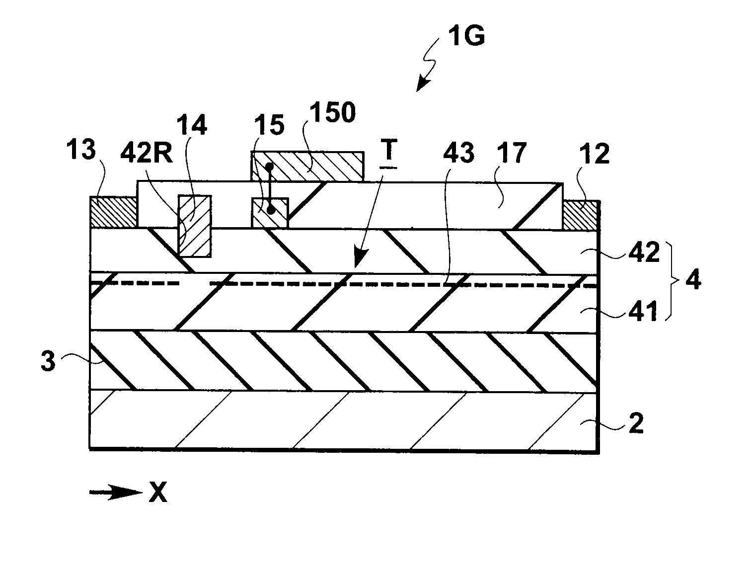
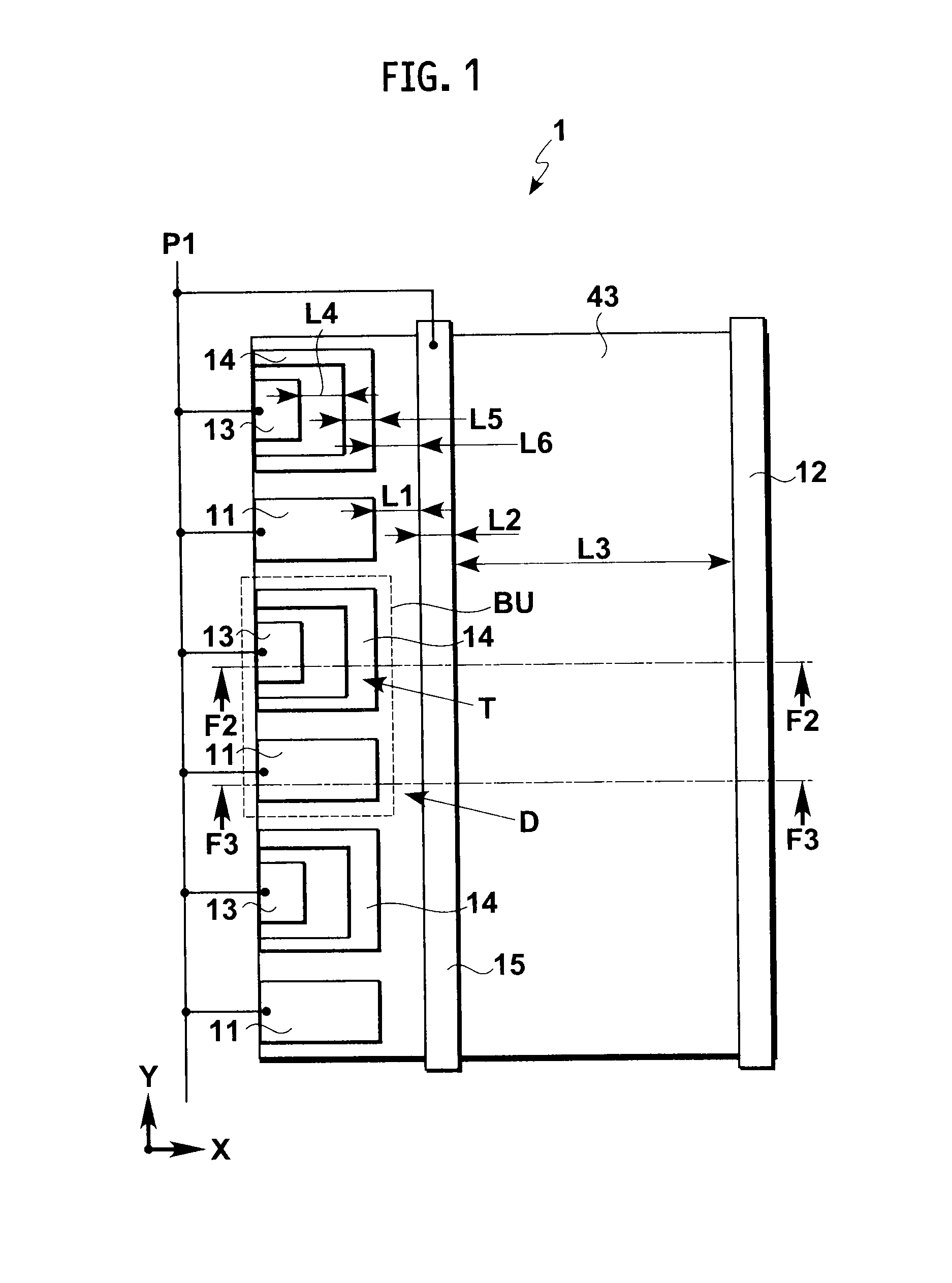
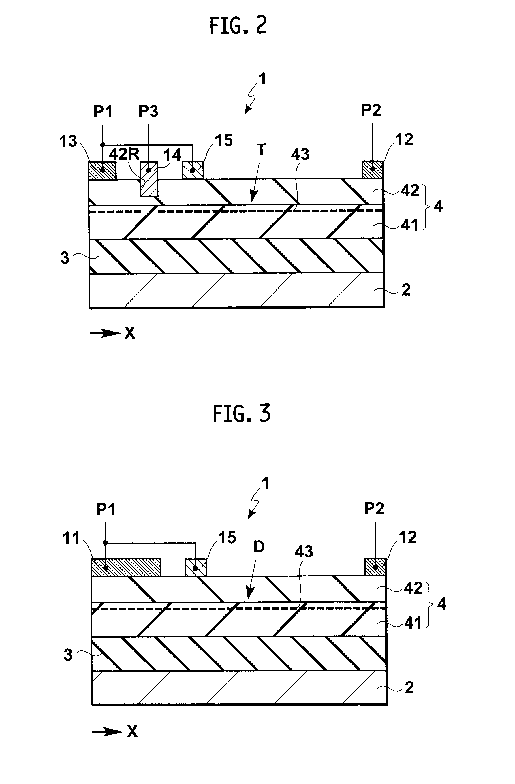
[0038]As illustrated in FIGS. 1 to 3, a semiconductor device 1 according to the first embodiment is a device in which the transistor T and the rectifier D are formed integrally with each other, and includes a current path 43, first main electrodes 11, a second main electrode 12, an auxiliary electrode 15, third main electrodes 13, and control electrodes 14. The first main electrodes 11 have a rectifying function, and are arranged on one end of the current rout 43 (that is, on a left side of the semiconductor device 1 in FIGS. 1 to 3). The second main electrode 12 is arranged on the other end of the current path 43 (that is, on a right side of the semiconductor device 1 in FIGS. 1 to 3). The auxiliary electrode 15 has the rectifyin...

second embodiment

[0068]A second embodiment of the present invention describes an example where, in the semiconductor device 1 according to the above-mentioned first embodiment, the reduction of the forward voltage of the rectifier D is further promoted.

[Device Structure of Semiconductor Device]

[0069]In a semiconductor device 1A according to the second embodiment, which is illustrated in FIG. 8, planar structures of the transistor T and the rectifier D are substantially the same as planar structures of the transistor T and the rectifier D in the semiconductor device 1 according to the above-mentioned first embodiment. Moreover, a cross-sectional structure of the transistor T is also substantially the same as a cross-sectional structure of each of the transistor T of the semiconductor device 1 according to the above-mentioned first embodiment. The semiconductor device 1A according to the second embodiment is different from the semiconductor device 1 in cross-sectional structure of the rectifier D.

[007...

third embodiment

[0072]A third embodiment of the present invention describes an example where the reduction of the forward voltage of the rectifier D is further promoted in a similar way to the semiconductor device 1A according to the above-mentioned second embodiment.

[Device Structure of Semiconductor Device]

[0073]As illustrated in FIGS. 9 and 10, in a semiconductor device 1B according to the third embodiment, a planar structure and cross-sectional structure of the transistor T are substantially the same as the planar structures and cross-sectional structures of the transistor T of the semiconductor devices 1 and 1A according to the above-mentioned first embodiment and second embodiment; however, the semiconductor device 1B is different from the semiconductor devices 1 and 1A particularly in planar structure and cross-sectional structure of the first main electrodes (anode electrode of the rectifier D) 11. Each of the first main electrodes 11 is composed of a composite electrode including a first s...


PUM


Abstract

A semiconductor device having a transistor and a rectifier includes: a current path; a first main electrode having a rectifying function and arranged on one end of the current path; a second main electrode arranged on the other end of the current path; an auxiliary electrode arranged in a region of the current path between the first main electrode and the second main electrode; a third main electrode arranged on the one end of the current path apart from the first main electrode along a direction intersecting the current path; and a control electrode arranged in a region of the current path between the second main electrode and the third main electrode. The transistor includes the current path, the second main electrode, the third main electrode, and the control electrode. The rectifier includes the current path, the first main electrode, the second main electrode, and the auxiliary electrode.

Description

BACKGROUND OF THE INVENTION[0001]1. Field of the Invention[0002]The present invention relates to a semiconductor device having a transistor and a rectifier.[0003]2. Description of the Related Art[0004]In recent years, a high electron mobility transistor (HEMT) using a gallium nitride (GaN)-based compound semiconductor has been used frequently. The GaN-based HEMT has a low resistance value and a high breakdown voltage, and accordingly, is frequently used for use in electric power, and specifically, for a power supply circuit.[0005]By Kinzer (U.S. Pat. No. 7,498,617 B2), a HEMT is disclosed, which includes an antiparallel diode that prevents noise of an opposite polarity voltage by introducing a reverse current. The HEMT disclosed by Kinzer has an object to prevent damage and breakage of the HEMT, which result from the noise of the opposite polarity voltage, by adding the antiparallel diode.[0006]The HEMT disclosed by Kinzer has heterojunction in which a first group III nitride semico...

Claims


Application Information

Patent Timeline
IPC IPC(8): H01L29/778
CPCH01L27/0605H01L29/2003H01L29/872H01L29/7787H01L29/42316
Inventor MACHIDA, OSAMUIWABUCHI, AKIO
Owner SANKEN ELECTRIC CO LTD
Why Eureka
Try Eureka