Semiconductor light-emitting device, light-emitting module, and illumination device

a technology of semiconductors and light-emitting devices, which is applied in semiconductor devices for light sources, point-like light sources, lighting and heating apparatuses, etc., can solve the problem of limiting the interval between led chips on printed wiring boards to be reduced, and achieve the effect of improving luminous efficiency

Active Publication Date: 2011-11-03
PANASONIC CORP
View PDF25 Cites 88 Cited by
  • Summary
  • Abstract
  • Description
  • Claims
  • Application Information

AI Technical Summary

Benefits of technology

[0016]In the semiconductor light-emitting device pertaining to the present invention having the stated structure, the first electrode is connected to the first conductive layer at the bottom of the hole provided in the center portion of the light-emitting element in plan view, and the second electrode is formed on the second conductive layer so as to surround the opening of the hole. Thus, between the first electrode and the second electrode, current flows in all directions from the first electrode in plan view. Therefore, the current flows are more uniform and spread wider in the light-emitting layer than the conventional semiconductor light-emitting device described above. That is, the current density in the light-emitting layer is made uniform as much as possible. This improves the luminous efficiency because the current density of the portion where is likely to have the highest current density is lower than the conventional semiconductor light-emitting device when provided with the same amount of current in total.

Problems solved by technology

However, there is a limit to how much the intervals between the LED chips on the printed wiring board can be reduced.

Method used


Image

  • Semiconductor light-emitting device, light-emitting module, and illumination device
  • Semiconductor light-emitting device, light-emitting module, and illumination device
  • Semiconductor light-emitting device, light-emitting module, and illumination device

Examples


embodiment 1

Structure of LED Array Chip

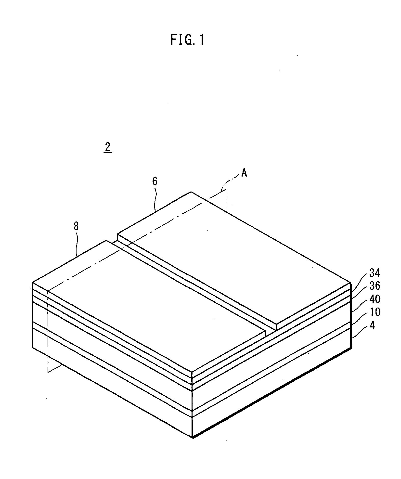
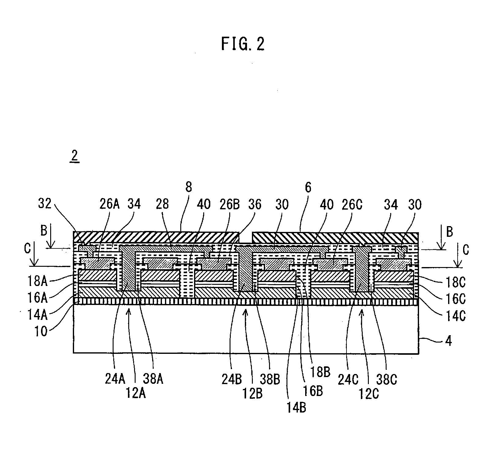
[0045]FIG. 1 is a perspective view showing an overall structure of an LED array chip 2 as a semiconductor light-emitting device, and FIG. 2 is a cross-sectional view of the LED array chip 2 cut along the plane A shown in FIG. 1. Note that the scale ratio between the elements is not the same in each of the drawings, including FIG. 1 and FIG. 2.

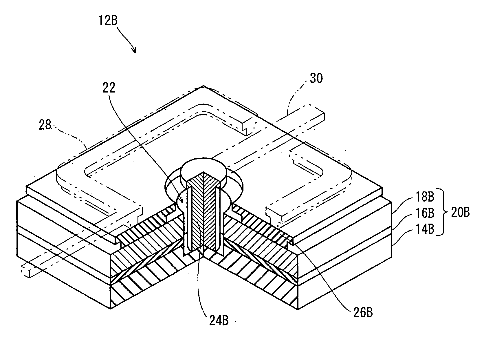
[0046]As shown in FIG. 1, the LED array chip 2 has a structure in which a plurality of LEDs as light-emitting elements (not depicted in FIG. 1) are disposed between an SiC substrate 4 or the like (hereinafter simply referred to as “SiC substrate 4”) and first and second power supply terminals 6 and 8. In this example, nine LEDs are disposed on the SiC substrate 4, as described below. In FIG. 1, note that a high-resistance layer 10 and insulating films (i.e. layers) 34, 36 and 40 are shown on the side surfaces of the LED array chip 2 sandwiched between the SiC substrate 4 and the first and second power supply terminals...

embodiment 2

Structure of LED Array Chip

[0109]The LED array chip 2 pertaining to Embodiment 1 has the nine LEDs, namely LEDs 12A-12I, and these LEDs are connected in a three-series three-parallel arrangement on the SiC substrate 4 (FIG. 5B). Instead of the SiC substrate, a substrate made of a translucent material, such as a GaN substrate, an aluminum nitride substrate and a ZnO substrate, may be used. Alternatively, a substrate having a wavelength conversion function, such as YAG:Ce, may be used.

[0110]In contrast, an LED array chip 200 pertaining to Embodiment 2 has 16 LEDs, namely LEDs 202A-202Q. As shown in FIG. 13A, the LEDs are arranged in groups W1, W2, W3 and W4 each including four LEDs. Each of the groups W1, W2, W3 and W4 are connected in two-series two-parallel arrangement, in which every two LEDs are serially connected, and these two sets of serially-connected LEDs are parallely connected such that they are opposite in polarity.

[0111]Each of the LEDs 202A-202Q has the same structure as...

embodiment 3

Structure of LED Array Chip

[0143]In Embodiments 1 and 2, each LED is composed of a semiconductor multilayer film having a square shape in plan view. In contrast, an LED array chip 300 pertaining to Embodiments 3, each LED is composed of a semiconductor multilayer film having a regular hexagonal shape in plan view. The width across corner is 2 [mm] in each chip, and is its ⅓ in each light-emitting element.

[0144]FIG. 21A shows a plan view of the LED array chip 300. Note that FIG. 21A shows only seven out of the LEDs 302A-302G formed on the SiC substrate 304 with the high-resistance layer 306 therebetween. The n-electrodes 308A-308G and the p-electrodes 310A-310G of the LEDs 302A-302G are depicted in two-dot chain lines.

[0145]FIG. 21B is a cross-sectional view of the LED array chip 300 cut along the line I-I in FIG. 21A.

[0146]All the LEDs 302A-302G have the same structure, and thus the LED 302G shown on the I-I cross section is explained as a representative. In Embodiment 3, as in Embo...


PUM

PropertyMeasurementUnit
resistivityaaaaaaaaaa
thicknessaaaaaaaaaa
thicknessaaaaaaaaaa

Abstract

A semiconductor light-emitting device having a substrate on which a semiconductor multilayer film is disposed, the semiconductor multilayer film having a layered structure in which a first conductive layer, a light-emitting layer and a second conductive layer are layered above the substrate from bottom to top in the stated order, and being divided into portions by grooves extending perpendicular to the substrate, each portion having a diode structure and serving as a light-emitting element 12, each light-emitting element 12 having a hole 22 in a central portion thereof in plan view, the hole 22 penetrating through the second conductive layer 18 and the light-emitting layer 16 and reaching the first conductive layer 14, and comprising: a first electrode 24 inserted in the hole 22 and having a columnar shape, one end thereof being connected to the first conductive layer 14 at the bottom of the hole 22, and the other end protruding from an opening of the hole 22; and a second electrode 26 formed on the second conductive layer 18 and having an annular shape surrounding the opening of the hole 22.

Description

TECHNICAL FIELD[0001]The present invention relates to semiconductor light-emitting devices, light-emitting modules and illumination apparatuses, and particularly relates to a semiconductor light-emitting device that includes a plurality of light-emitting elements.BACKGROUND ART[0002]A light-emitting diode (LED), which is a type of semiconductor light-emitting element, is smaller and exhibits higher efficiency than other light sources that utilize discharge or radiation. In addition, recent improvements in luminous flux of LEDs have been expanding the range of application thereof, from conventional displaying use to lighting use.[0003]In particular, bulb-type LED lamps that are attachable to sockets for conventional incandescent light bulbs and the likes have been introduced as alternatives to the conventional light bulbs.[0004]Meanwhile, the related supply voltage of a conventional light bulb is generally 100 [V], 24 [V] or 12 [V], whereas the drive voltage of a Single LED is in the...

Claims


Application Information

Patent Timeline
Patent Type & Authority Applications(United States)
IPC IPC(8): H01L33/50
CPCH01L27/156H01L33/20H01L33/382H01L2933/0016H01L2224/13F21V3/0418F21V3/0436F21Y2101/02F21K9/1355F21K9/23F21Y2115/10F21V3/062F21V3/061
Inventor NAGAI, HIDEO
Owner PANASONIC CORP
Why Eureka
Try Eureka