Backside-illuminated sensor with noise reduction

a backside illumination and sensor technology, applied in the field of image sensors, can solve the problems of quantum efficiency, difficult to achieve certain functionalities, cross-talk and dark current in the sensor array, and the degradation resulting from certain factors, so as to achieve the effect of simple noise reduction element and efficient noise reduction

Inactive Publication Date: 2011-11-17
HIMAX IMAGING LIMITED
View PDF2 Cites 7 Cited by
  • Summary
  • Abstract
  • Description
  • Claims
  • Application Information

AI Technical Summary

Benefits of technology

[0006]In light of this, the present invention provides a backside-illuminated (BSI) sensor with a simple noise reduction element capable of efficiently reducing noise.

Problems solved by technology

As the pixel size of a complementary metal-oxide-semiconductor image sensor (CMOS image sensor, CIS) grows smaller, the degradation resulting from certain factors such as quantum efficiency, cross-talk and dark current in a sensor array also becomes significant.
As a result, only a few spaces can be utilized for routing traces on the metal layers, and therefore certain functionalities, such as noise reduction and voltage regulation, are hard to achieve.

Method used


Image

  • Backside-illuminated sensor with noise reduction
  • Backside-illuminated sensor with noise reduction
  • Backside-illuminated sensor with noise reduction

Examples


Embodiment Construction

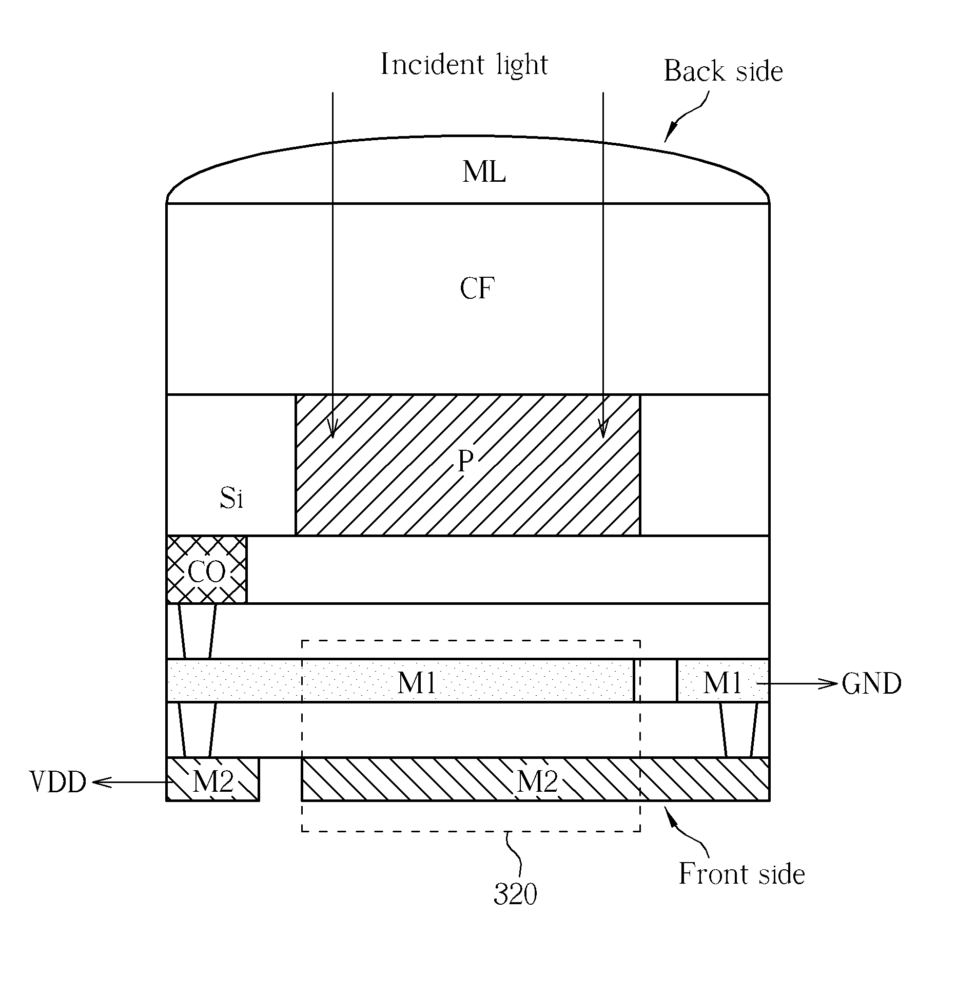
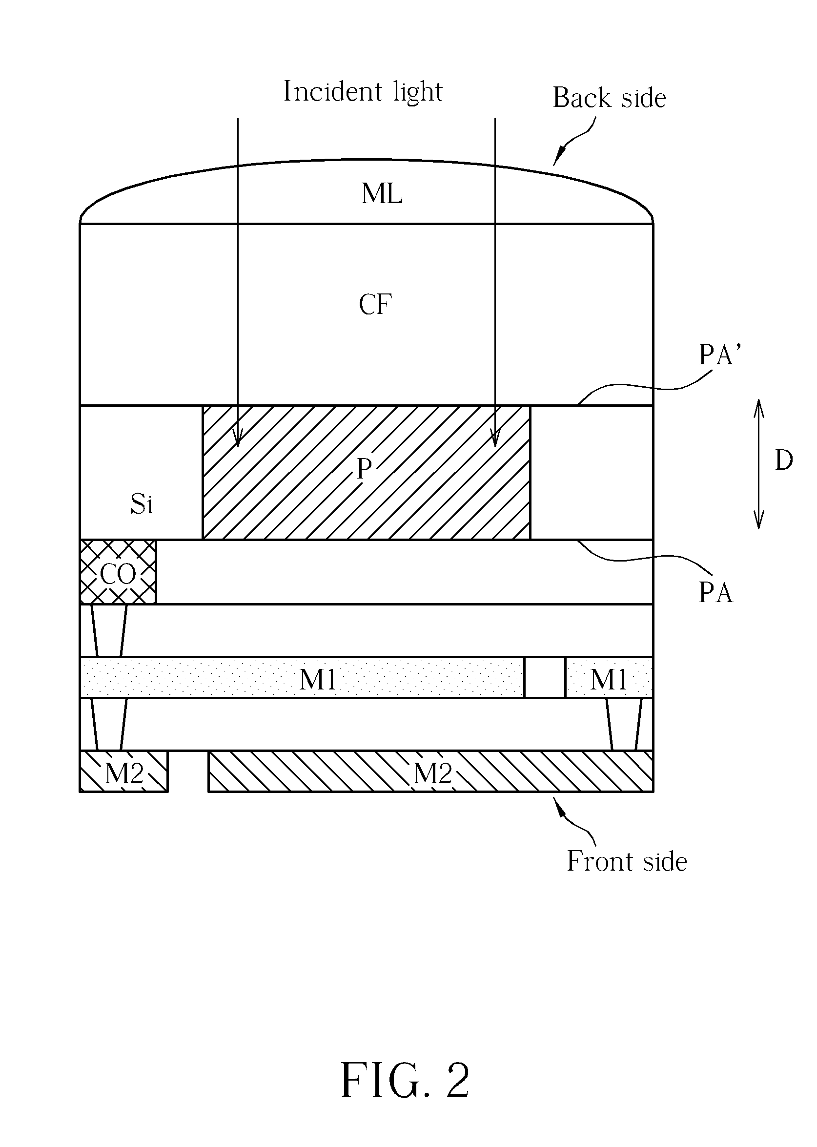
[0015]Please refer to FIG. 2, which is a cross-section view of a pixel structure of a backside illuminated (BSI) sensor array according to an embodiment of the present invention. As shown in FIG. 2, an incident light travels through a micro lens ML, a color filter CL, and ends up being projected directly onto a photo diode Pin the substrate Si. Since the incident light is projected from the backside of the substrate Si, the metal layers M1, M2 and other circuitries are on the opposite side of the substrate Si and are much easier to have traces routed thereon. Therefore, the metal layers M1 and M2 can be utilized to improve the overall sensing performance.

[0016]Please refer to FIG. 3, which is a circuit diagram of a pixel structure 300 according to an embodiment of the present invention. The pixel structure 300 is formed on a pixel area PA included in a front surface of the substrate Si. Due to the BSI sensor structure, a projected area PA′ of the pixel area PA on a backside surface ...


PUM


Abstract

A backside-illuminated sensor includes a substrate, at least one lens and at least one pixel structure. The substrate has a front surface and a backside surface, and the lens is formed on the backside surface of the substrate and the pixel structure is formed on a pixel area included in the front surface of the substrate, where a projected area of the pixel area on the backside surface in a thickness direction of the substrate is covered by the lens. The pixel structure includes a first power node for receiving a first supply voltage, a second power node for receiving a second supply voltage different from the first supply voltage, a sensing element and a capacitor for noise reduction. The sensing element generates a sensing signal according to an incident luminance from the lens.

Description

BACKGROUND OF THE INVENTION[0001]1. Field of the Invention[0002]The present invention relates to an image sensor, and more particularly, to a backside-illuminated sensor with noise reduction.[0003]2. Description of the Prior Art[0004]As the pixel size of a complementary metal-oxide-semiconductor image sensor (CMOS image sensor, CIS) grows smaller, the degradation resulting from certain factors such as quantum efficiency, cross-talk and dark current in a sensor array also becomes significant. Regarding a conventional image sensor such as a front side illuminated sensor, a lens of each pixel sensor is fabricated on a front side of a substrate. Therefore, the incident light has to travel through dielectric layers between circuitry formed by metal layers to arrive at a photo diode, or the traveling light will be reflected or absorbed by metal or any other reflective material. Since the traveling path of light cannot be blocked by metal or any other kind of reflective material, there is ...

Claims


Application Information

Patent Timeline
Patent Type & Authority Applications(United States)
IPC IPC(8): H01L31/0232H01L31/00
CPCH01L27/14621H01L27/14627H01L27/14636H01L27/14641H01L28/86H01L27/1464H01L27/14643
Inventor HUANG, FANG-MINGYIN, PING-HUNGCHANG, CHUNG-WEI
Owner HIMAX IMAGING LIMITED
Why Eureka
Try Eureka