Chip-Exposed Semiconductor Device and Its Packaging Method

Active Publication Date: 2011-11-24
ALPHA & OMEGA SEMICON INC
View PDF2 Cites 10 Cited by
  • Summary
  • Abstract
  • Description
  • Claims
  • Application Information

AI Technical Summary

Benefits of technology

[0032]The semiconductor device as provided in the invention has no external leads extending beyond the package body, therefore the additional space for accommodating the external

Problems solved by technology

Unfortunately certain parameters have to be sacrificed in order to meet the specification of others due to the nature they are competing with each other.
In general small footprint usually means small chip size and small heat dissipation su

Method used


Image

  • Chip-Exposed Semiconductor Device and Its Packaging Method
  • Chip-Exposed Semiconductor Device and Its Packaging Method
  • Chip-Exposed Semiconductor Device and Its Packaging Method

Examples


Example

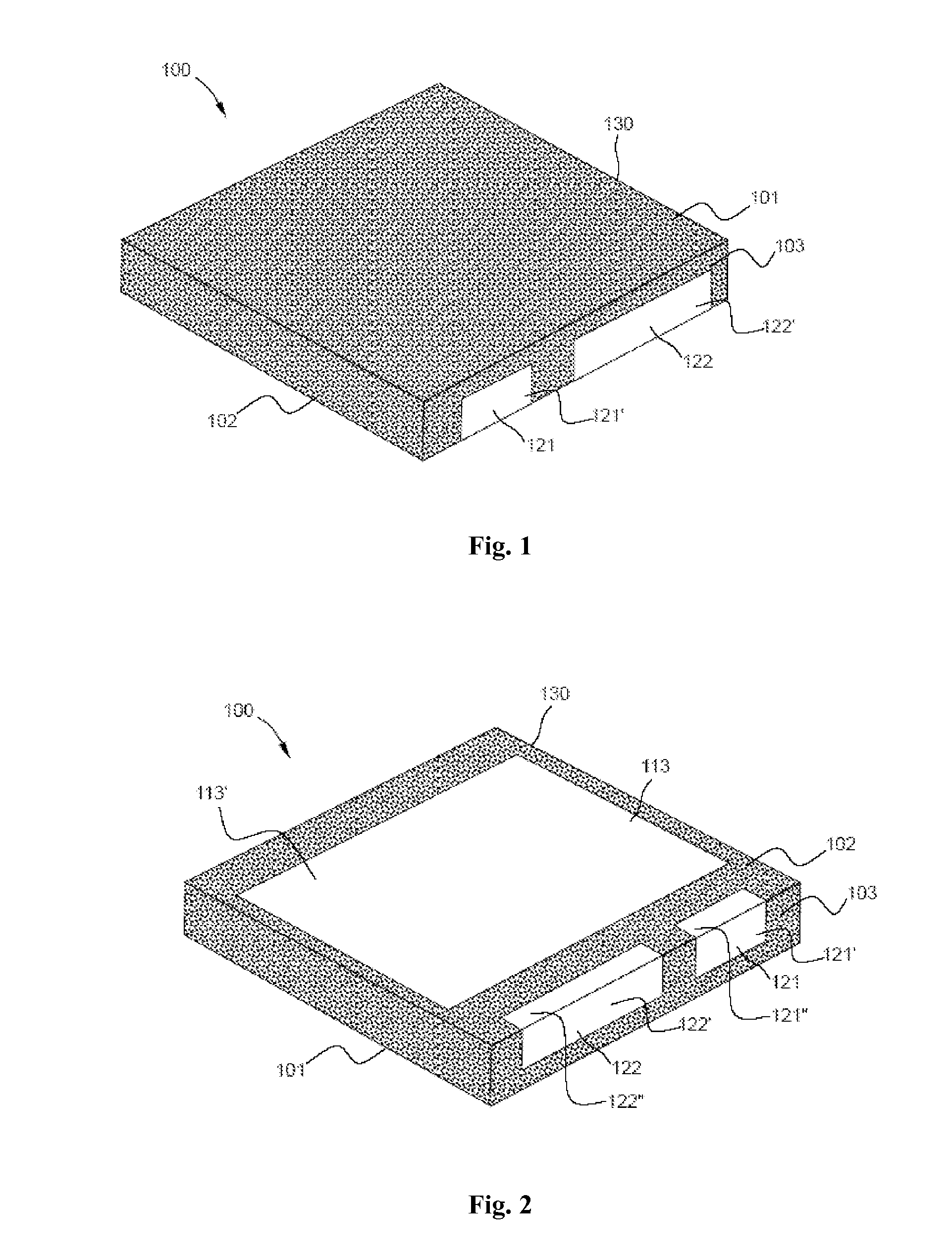
[0040]FIG. 1 is a top view of a semiconductor device according to this invention. The semiconductor device 100 is a none-lead package with a package body 130 including a top surface 101, a bottom surface 102 and a sidewall 103 perpendicular to the bottom surface 102. A side faces 121′ of a gate terminal 121 and a side face 122′ of a source terminal 122 of the semiconductor device 100 exposed on the sidewall 103.

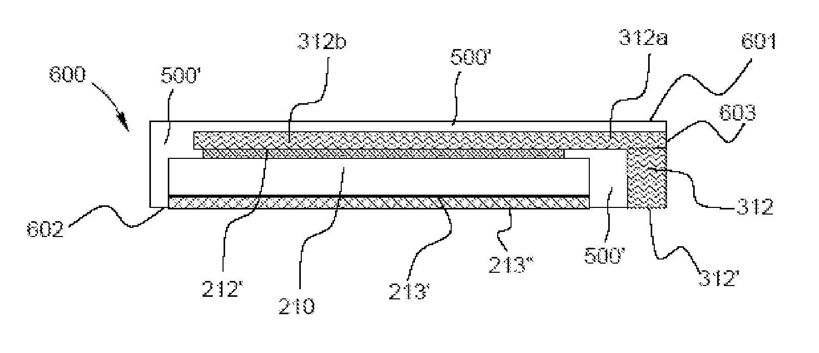
[0041]As shown in FIG. 2 a bottom view of a semiconductor device 100, a backside metal layer 113, a bottom 121″ of the gate terminal 121 and a bottom 122″ of the source terminal 122 are exposed on the bottom surface 102 of the package body 130.

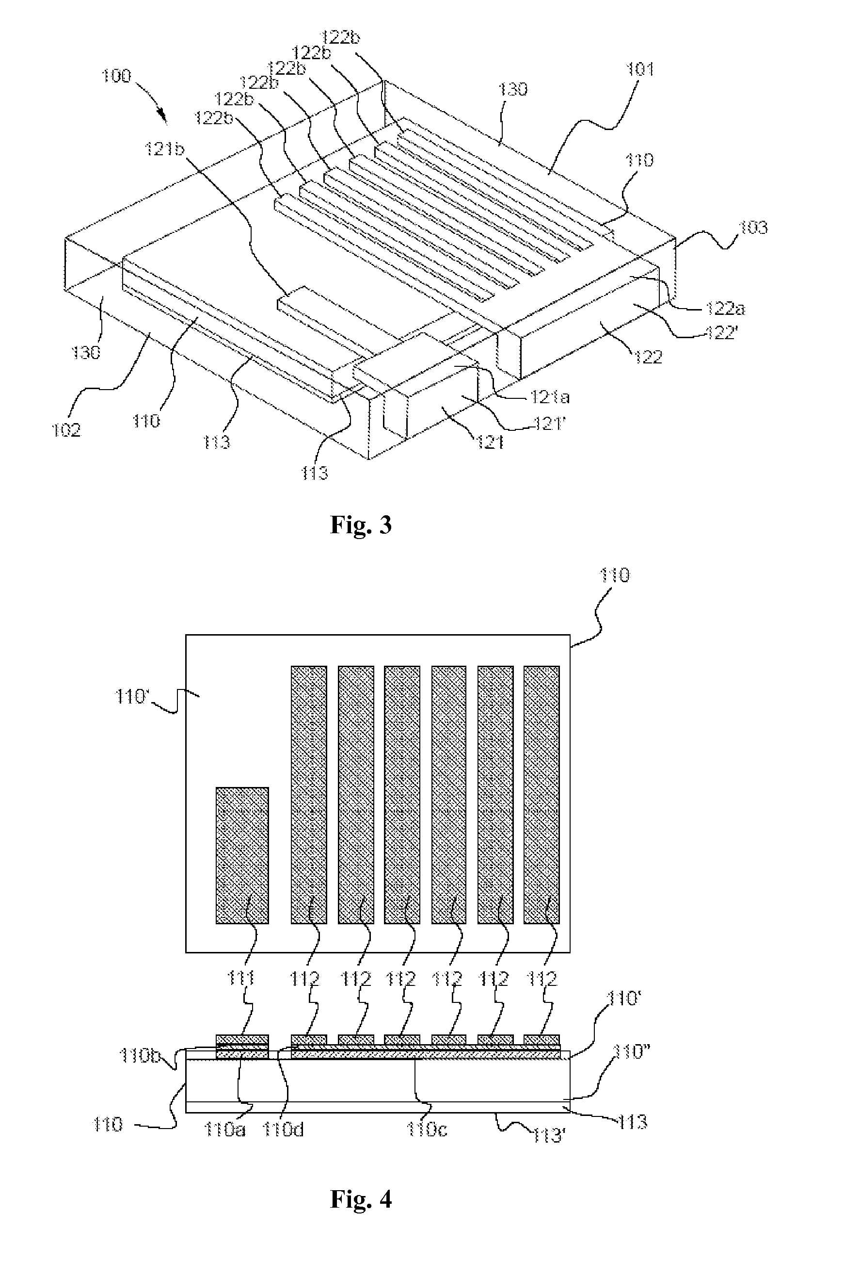
[0042]As shown in a perspective structure view FIG. 3 of the semiconductor device 100, a semiconductor chip 110 is molded and encapsulated in the package 130, wherein the package body 130 is generally made of solidified epoxy molding compound. By way of example but not limitation, the semiconductor chip 110 may be a vertical MOSFET chip...


PUM


Abstract

A method of making a chip-exposed semiconductor package comprising the steps of: plating a plurality of electrode on a front face of each chi on a wafer; grinding a backside of the wafer and depositing a back metal then separating each chips; mounting the chips with the plating electrodes adhering onto a front face of a plurality of paddle of a leadframe; adhering a tape on the back metal and encapsulating with a molding compound; removing the tape and sawing through the leadframe and the molding compound to form a plurality of packaged semiconductor devices.

Description

CROSS REFERENCE TO OTHER APPLICATIONS[0001]This application is a continuation in part of co-pending U.S. patent application Ser. No. 12 / 786,328 (Attorney Docket No. APOM043) entitled “A Wafer Level Chip Scale Package Method Using Clip Array” filed May 24, 2010, which is incorporated herein by reference for all purpose.BACKGROUND OF THE INVENTION[0002]1. Technical Field[0003]The present invention relates to a semiconductor device package, and more specifically, to a chip-exposed semiconductor device without extending leads and its production method.[0004]2. Description of the Related Art[0005]Surface mounted technology (SMT) is commonly used to mount electronic component on the printed circuit board (PCB). Power handling capacity, heat dissipation and device size are the important parameters in selecting semiconductor power device for SMT applications. It is desirable to produce a semiconductor power device capable of delivering high power with excellent heat dissipation, smaller foo...

Claims


Application Information

Patent Timeline
IPC IPC(8): H01L23/498H01L21/60
CPCH01L21/568H01L23/3107H01L2224/3701H01L2924/1816H01L2224/97H01L2224/94H01L2224/83191H01L2224/32245H01L2224/29339H01L2224/2929H01L2224/06181H01L23/49503H01L23/49548H01L23/49562H01L24/34H01L2924/01013H01L2924/01029H01L2924/01078H01L2924/01082H01L2924/01005H01L2924/01033H01L2924/01047H01L2924/014H01L2924/13091H01L24/03H01L24/05H01L24/06H01L24/29H01L24/32H01L24/83H01L24/97H01L2224/0346H01L2224/05611H01L2224/05639H01L2924/01028H01L2224/03H01L2224/27H01L2224/83H01L2224/0603H01L2924/181H01L2224/40245H01L24/40H01L24/37H01L2224/371H01L2224/8485H01L2924/00012
Inventor GONG, YUPINGXUE, YAN XUN
Owner ALPHA & OMEGA SEMICON INC
Why Eureka
Try Eureka