Electrode for plasma processes and method for manufacture and use thereof

a plasma process and electrode technology, applied in the direction of plasma technique, chemical vapor deposition coating, coating, etc., can solve the problems of excessive electrode wear, metallurgical bond failure at high plasma processing power, electrode warpage, etc., to reduce heat generation, reduce build-up, and reduce the effect of rf power

Inactive Publication Date: 2002-09-12
LAM RES CORP
View PDF1 Cites 112 Cited by
  • Summary
  • Abstract
  • Description
  • Claims
  • Application Information

AI Technical Summary

Benefits of technology

0015] In a preferred plasma etching process, the electrode can comprise an RF driven single crystal silicon showerhead electrode bonded or clamped to a temperature-controlled member through which the process gas is supplied to the showerhead electrode. The RF driven electrode can form the plasma by energizing the process gas and the substrate can comprise a silicon wafer which is subjected to etching by the plasma. The electrode can also comprise an electrically grounded, non-powered single crystal silicon showerhead electrode bonded or clamped to a temperature-controlled member through which the process gas is supplied to the showerhead electrode. The grounded showerhead electrode can provide a ground path effective to confine the plasma and the substrate can comprise a silicon wafer which is subjected to etching by the plasma.
0016] In use, the electrode according to the invention can couple RF power into the plasma more efficiently and with less heat-up compared to a conventional electrode having an electrical resistivity of 10 ohm-cm or higher. Further, in the case where the electrode according to the invention includes gas outlets through which the process gas passes into the chamber wherein the gas outlets have diameters of 0.020 to 0.030 inch and the process gas comprises an etchant gas, the electrode can exhibit less build-up of polymer byproducts within the gas outlets and on a backside of the electrode during etching of the substrate with the etchant gas compared to a conventional electrode having 0.033 inch diameter gas outlets.

Problems solved by technology

It has been found that metallurgical bonds such as In bonds cause the electrode to warp due to differential thermal expansion / contraction of the electrode and the part to which the electrode is bonded.
It has also been found that these metallurgical bonds fail at high plasma processing powers due to thermal fatigue and / or melting of the bond.
However, many chemically active agents have been found to cause excessive electrode wear.

Method used


Image

  • Electrode for plasma processes and method for manufacture and use thereof
  • Electrode for plasma processes and method for manufacture and use thereof
  • Electrode for plasma processes and method for manufacture and use thereof

Examples


Embodiment Construction

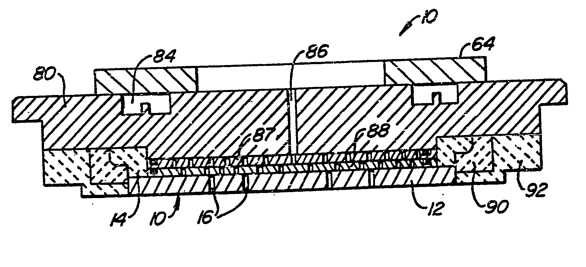
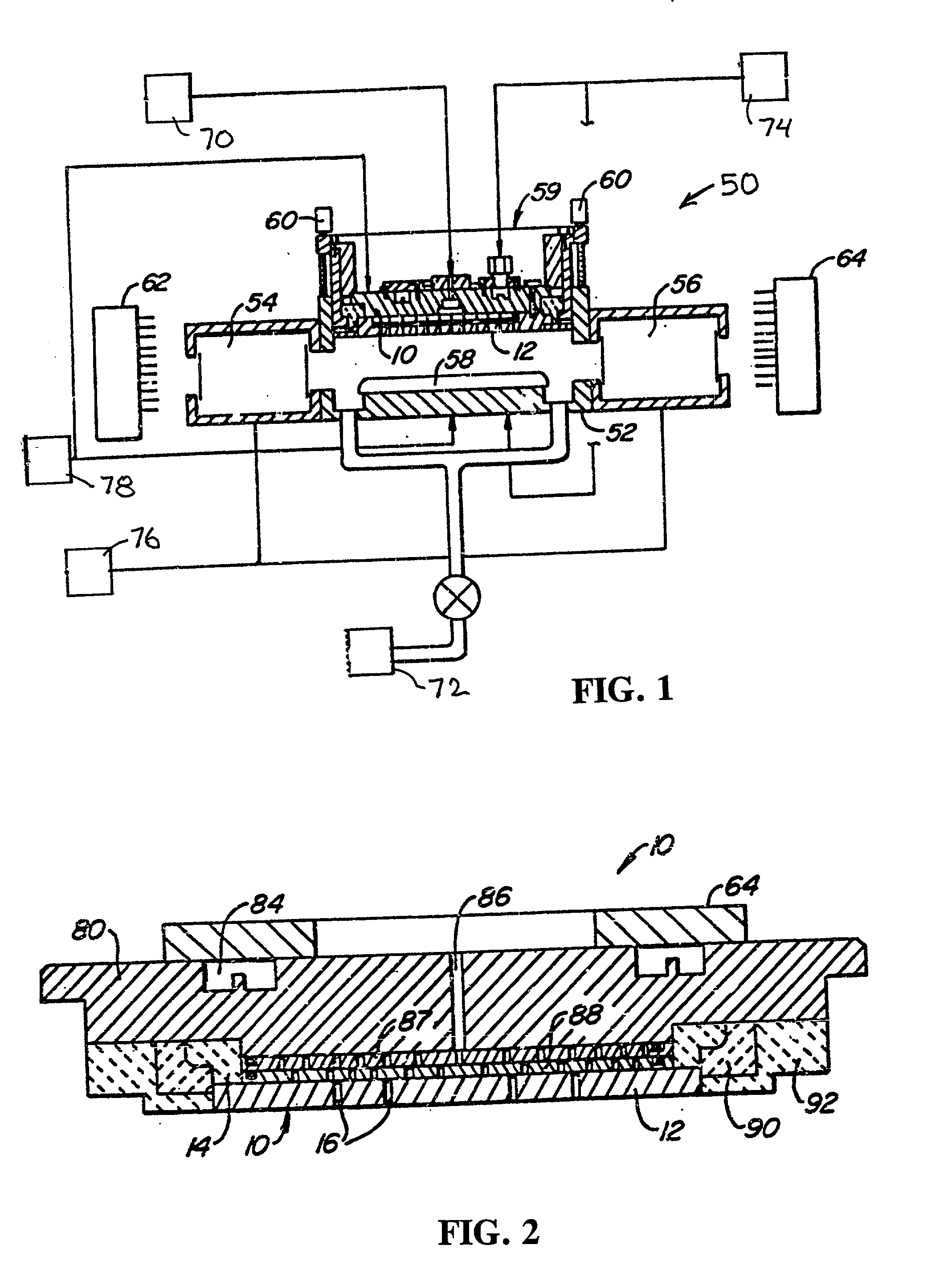
[0025] The invention provides a low resistivity silicon electrode which has advantages over conventional higher resistivity electrodes used in plasma reactors by providing improved impedance to ground which improves plasma confinement, improved plasma processing such as increased etching rate while maintaining etch rate uniformity, and / or improved temperature control by minimizing heat-up and reducing ohmic losses whereby power can be more efficiently coupled into the plasma.

[0026] It has been found that the silicon electrode according to the invention provides unexpected improvement in plasma processing of semiconductor substrates such as silicon wafers, particularly during plasma etching compared to conventional electrodes. For purposes of explanation, the electrode according to the invention will be described with reference to a showerhead electrode useful in plasma processing of semiconductor substrates.

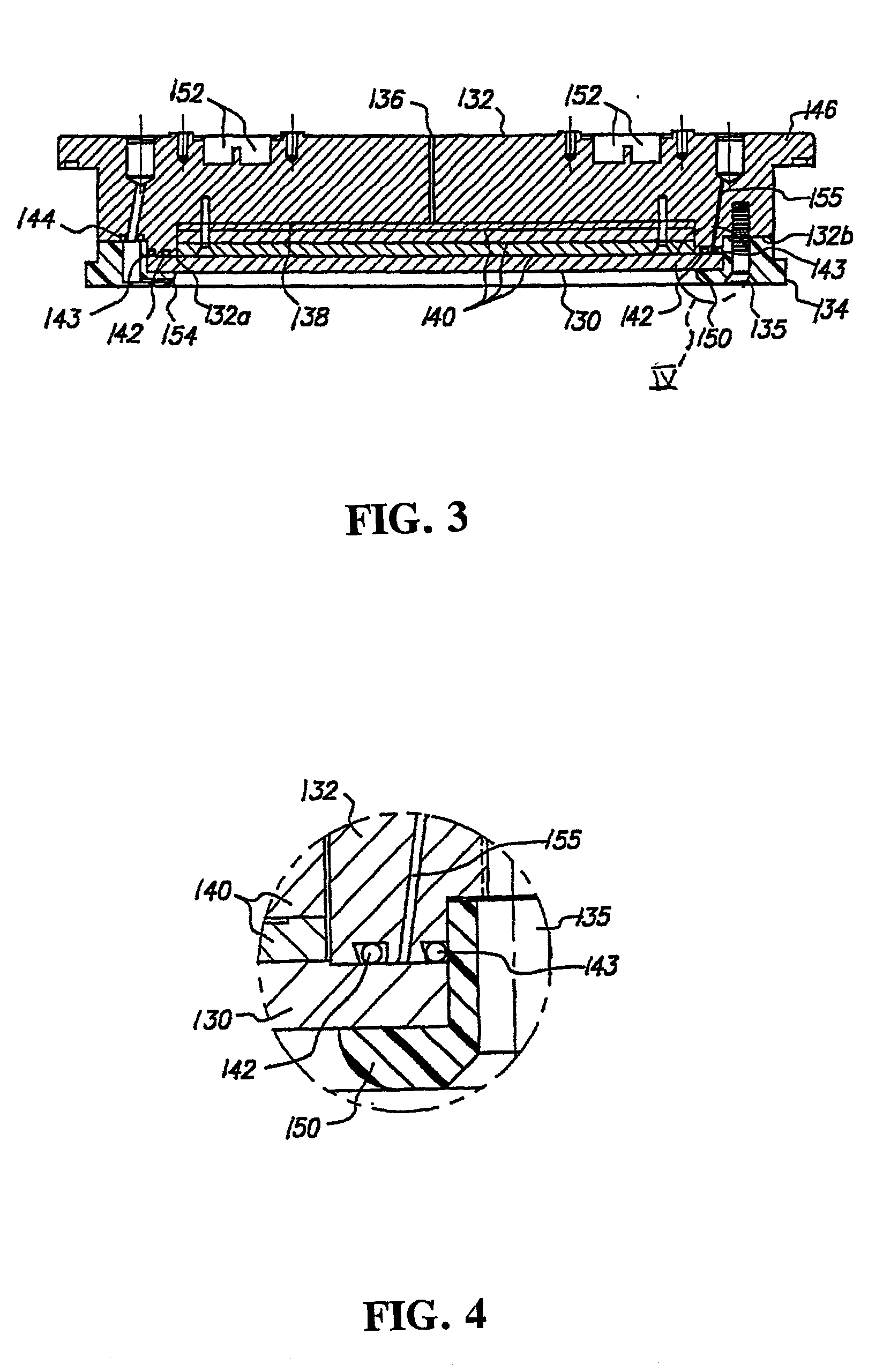
[0027] According to a preferred embodiment of the invention, a low resistivi...


PUM

PropertyMeasurementUnit
diametersaaaaaaaaaa
diameteraaaaaaaaaa
diameteraaaaaaaaaa

Abstract

A silicon electrode for a plasma reaction chamber wherein processing of a semiconductor substrate such as a single wafer can be carried out and a method of processing a semiconductor substrate with the electrode. The electrode is a low resistivity electrode having an electrical resistivity of less than 1 ohm-cm. The electrode can be a zero defect single crystal silicon or silicon carbide electrode such as a showerhead electrode bonded or clamped to support such as a temperature controlled plate or ring. The showerhead electrode can be in the form of a circular disk of uniform thickness and an elastomeric joint can be provided between a support ring and the electrode. The electrode can include gas outlets having 0.020 to 0.030 inch diameters.

Description

BACKGROUND OF THE INVENTION[0001] 1. Field of the Invention[0002] The invention relates to an apparatus for plasma processing of semiconductor substrates such as silicon wafers, and more particularly, to an electrode assembly having a low resistivity electrode. The invention also relates to processing semiconductor substrates with the electrode assembly.[0003] 2. Description of the Related Art[0004] Electrodes used in plasma processing reactors for processing semiconductor substrates such as silicon wafers are disclosed in U.S. Pat. Nos. 5,074,456 and 5,569,356, the disclosures of which are hereby incorporated by reference. The '456 patent discloses an electrode assembly for a parallel plate reactor apparatus wherein the upper electrode is of semiconductor purity and bonded to a support frame by adhesive, solder, or brazing layer. The soldering or brazing layer can be low vapor pressure metals such as indium, silver and alloys thereof and the bonded surfaces of the support frame and...

Claims


Application Information

Patent Timeline
Patent Type & Authority Applications(United States)
IPC IPC(8): H05H1/46H01J37/32H01L21/3065
CPCH01J37/32009H01J37/3255H01L21/3065
Inventor HUBACEK, JEROME S.ELLINGBOE, ALBERT R.BENZING, DAVID
Owner LAM RES CORP
Why Eureka
Try Eureka