Light Emitting Device Using AC and Manufacturing Method of the Same

a technology of light emitting devices and manufacturing methods, which is applied in the direction of transit-tube circuit elements, cathode-ray/electron beam tube circuit elements, lighting and heating apparatus, etc., can solve the problems of affecting the flexibility of led installation and use, and achieve the effect of high luminan

Inactive Publication Date: 2011-11-24
APT ELECTRONICS
View PDF6 Cites 18 Cited by
  • Summary
  • Abstract
  • Description
  • Claims
  • Application Information

AI Technical Summary

Benefits of technology

[0009]One purpose of the present invention is to overcome shortcomings and drawbacks in the prior art and provide a light emitting device which can directly use AC power source and exhibit a high luminance.

Problems solved by technology

However, an LED requires supply of DC power source.
However, these external devices all need to occupy partial space of the LED light source and affect flexibility in the installation and use of the LED.

Method used


Image

  • Light Emitting Device Using AC and Manufacturing Method of the Same
  • Light Emitting Device Using AC and Manufacturing Method of the Same
  • Light Emitting Device Using AC and Manufacturing Method of the Same

Examples


embodiment 1

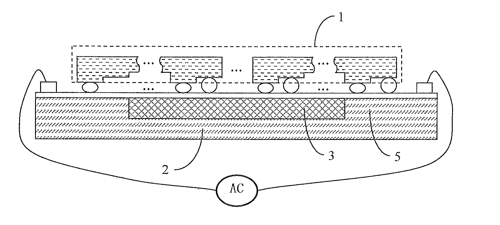
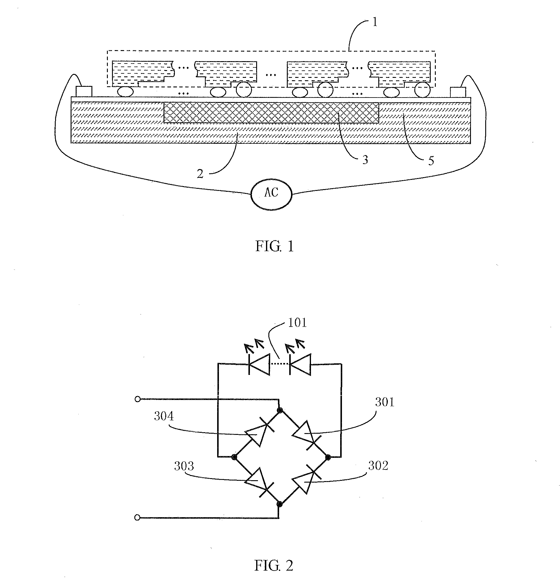
[0058]Referring to FIG. 2, it is a schematic view of a circuit of a first embodiment of the light emitting device using AC according to the present invention. The rectifying circuit 3 comprises a first diode 301, a second diode 302, a third diode 303 and a fourth diode 304. The first diode 301 and the fourth diode 304 are connected in series to form a first branch, the second diode 302 and the third diode 303 are connected in series to form a second branch, and the first branch and the second branch are connected in parallel to form an AC / DC bridge rectifier. The first branch and the second branch, after being connected in parallel, are connected in series with each light emitting region 101 in the LED chip 1. A connection point between the first diode 301 and the fourth diode 304, and a connection point between the second diode 302 and the third diode 303 are respectively electrically connected to the power source connecting terminals on the substrate 2 of the AC driving circuit ch...

embodiment 2

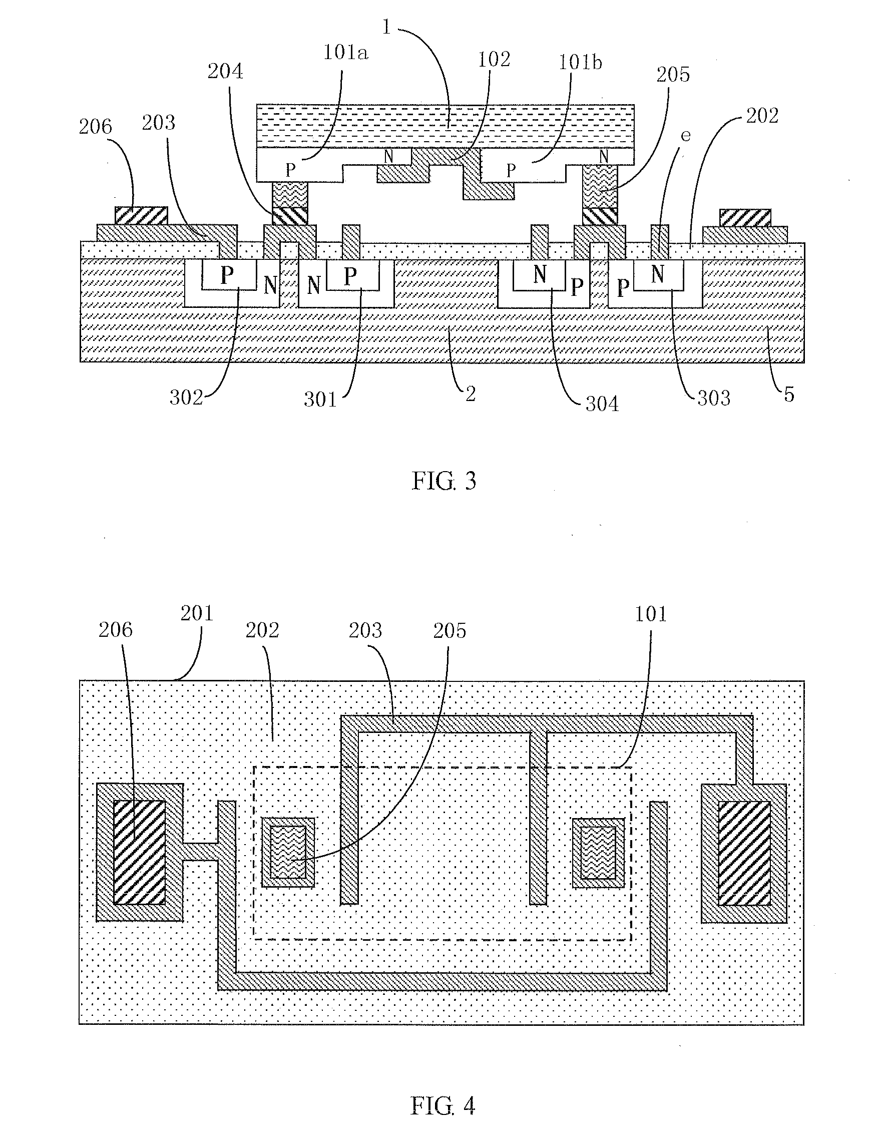
[0073]Simultaneously referring to FIG. 5 and FIG. 6, FIG. 5 is a cross-sectional view of a second embodiment of the light emitting device according to the present invention, and FIG. 6 is a top view of a surface of a substrate of the light emitting device shown in FIG. 5.

[0074]The light emitting device according to Embodiment 2 is structurally substantially the same as that in Embodiment 1. The same rectifying circuit 3 is integrated on the substrate 2. The only difference between the two embodiments is that the P electrode and N electrode of the light emitting region 101 on the light emitting diode chip 1 are both connected to the metal bump 205 of the substrate 2 by flip-chip, i.e., adjacent N electrode and P electrode in two adjacent light-emitting regions 101 are respectively connected to the metal bump 205 at a corresponding position of the upper surface of the substrate 2, and achieve in-series connection through the first metal wire layer 203 on the substrate 2.

[0075]A method...

embodiment 3

[0085]Referring to FIG. 7, FIG. 7 is a schematic view of a circuit of the light emitting device using AC according to a third embodiment of the present invention. The circuit of the light emitting device comprises a plurality of LED chips 103, a rectifying circuit 3 and a filter circuit 4. The plurality of LED chips 103 are mutually connected in series. The filter circuit 4 comprises a resistor 401 and a capacitor 402 connected in parallel. The rectifying circuit 3 is a bridge rectifying circuit which is structured the same as the rectifying circuit of Embodiment 1. The filter circuit 4 is connected in series at a power source input end of the rectifying circuit 3. The plurality of LED chips 103 connected in series are connected in series at an output end of the rectifying circuit 103.

[0086]Referring to FIG. 8 and FIG. 9, FIG. 8 is a cross-sectional view of the light emitting device according to the third embodiment of the present invention, and FIG. 9 is a top view on surface of th...


PUM


Abstract

The present invention relates to a light emitting device using AC, comprising: at least one LED chip and an AC driving circuit chip, wherein the AC driving circuit chip comprises a substrate and a rectifying circuit integrated on the substrate. The LED chip is flipped and bonded on the AC driving circuit chip by flip-chip technology and electrically connected to the rectifying circuit, and the AC driving circuit chip converts the AC into DC for supply to the LED chip. The present invention further relates to a method of manufacturing the light emitting device using AC, comprising the following steps of: (1) forming an LED chip; (2) integrating a rectifying circuit on a substrate, forming two power source connecting terminals on the substrate, and forming an AC driving circuit chip; and (3) flip-chip bonding the LED chip on the AC driving circuit chip and in electrical connection with the rectifying circuit on the substrate. The light emitting device according to the present invention can be used by being directly connected to AC without needing any external integrated circuit device or electronic parts, thereby saving the assembling space and improving flexibility in use and meanwhile enhancing use efficiency of the light emitting regions.

Description

CROSS-REFERENCE TO RELATED APPLICATION[0001]This application claims the benefit of the filing date of Chinese Application No. CN 201010190052.1 filed May 24, 2010, the entire disclosure of which is incorporated herein by reference.FIELD OF THE INVENTION[0002]The present invention belongs to the field of manufacture of light emitting devices, relates to a structure of a light emitting device and a manufacturing method thereof, particularly to a light emitting device directly using alternating current (AC) and a manufacturing method thereof.BACKGROUND OF THE INVENTION[0003]Light-emitting diodes (LEDs) are advantageous in high efficiency, long service life and free of hazardous substances such as Hg. In the recent several years, with rapid improvement of the performances such as brightness and service life of the LEDs and decreasing of cost, LEDs are applied to more and more fields, including outdoor lighting such as street lamps, indoor lighting, and decorative lights etc.[0004]The co...

Claims


Application Information

Patent Timeline
Patent Type & Authority Applications(United States)
IPC IPC(8): F21V23/00H01L33/48H05B44/00
CPCH01L25/0753H01L25/167H01L2224/16Y02B20/348H05B33/0821H05B45/40Y02B20/30
Inventor ZHOU, YUGANGZENG, ZHAOMINGLAI, YIN HINGKEUNG, CHI WINGXU, CHAOJUNWANG, RUIZHENXIAO, GUOWEI DAVID
Owner APT ELECTRONICS
Why Eureka
Try Eureka