

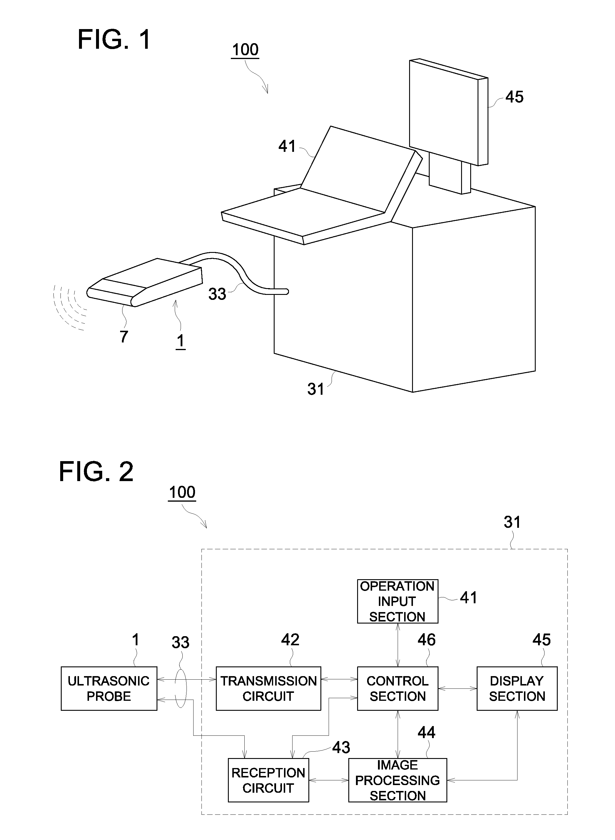
Ultrasonic probe and ultrasonic diagnostic device
- Summary
- Abstract
- Description
- Claims
- Application Information
AI Technical Summary
Benefits of technology
Problems solved by technology
Method used
Image

Examples
example 1
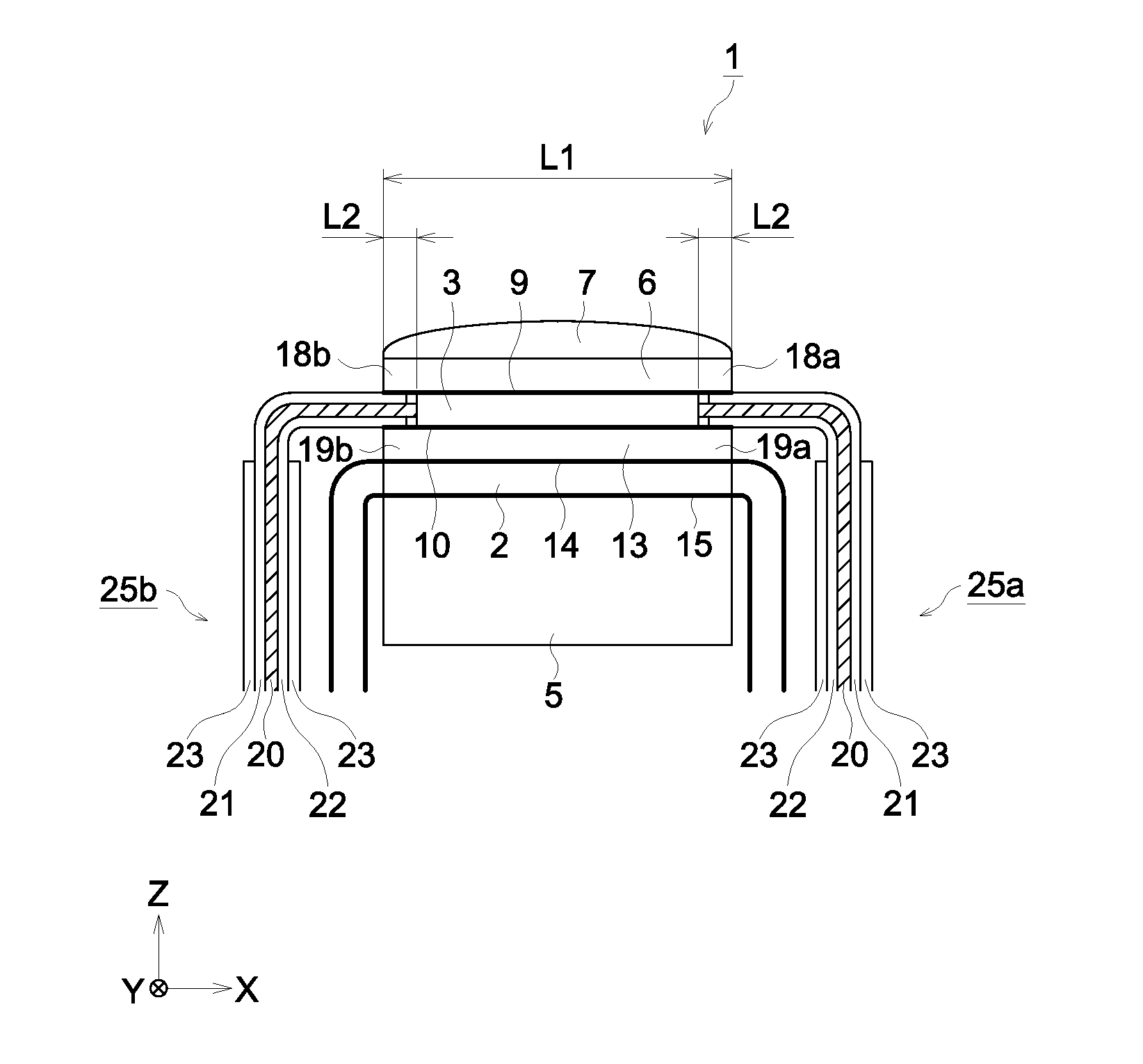
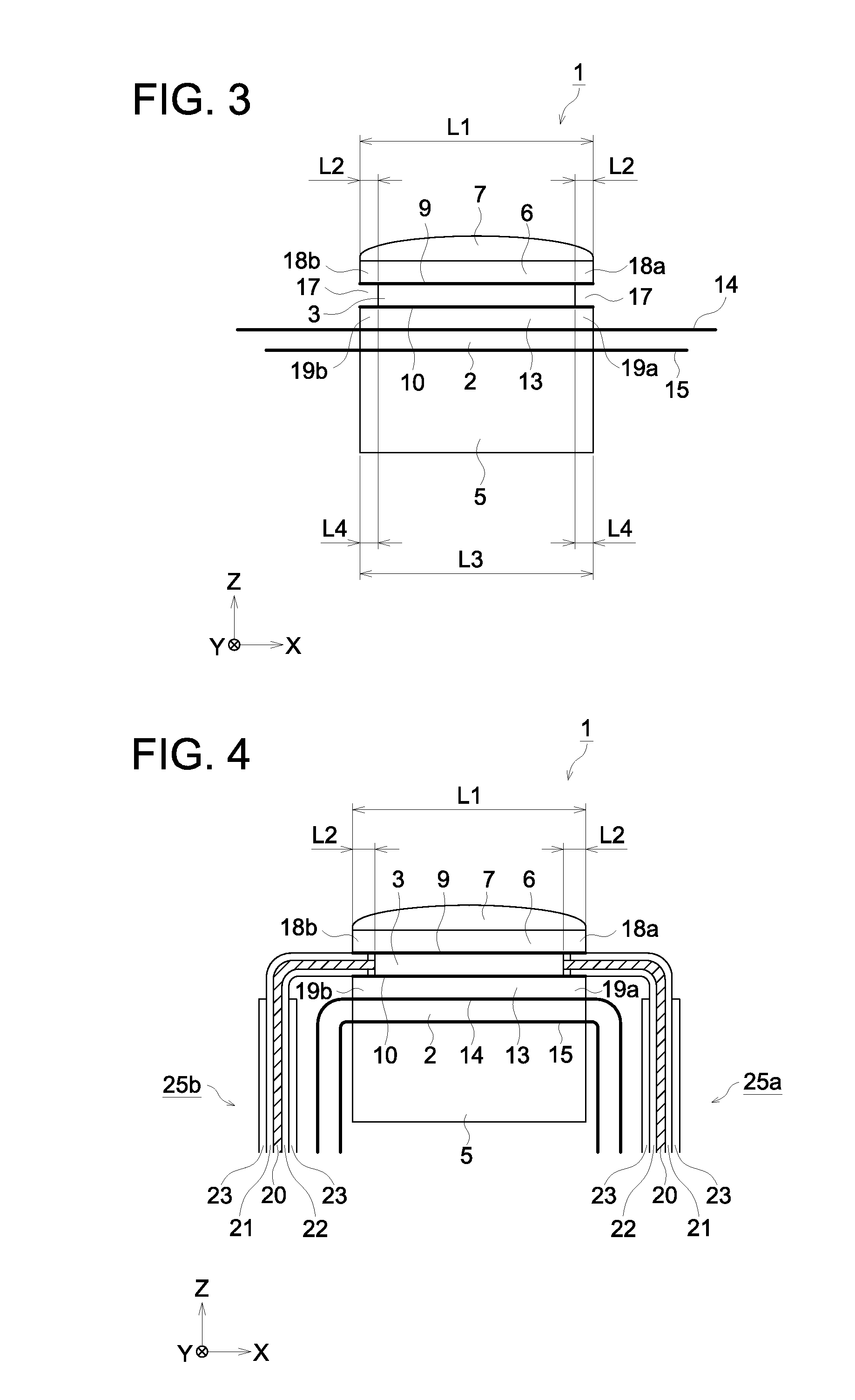
[0104]A hundred ultrasonic probes 1 having a structure shown in FIG. 3 were manufactured by changing the length of the reception element layer 3 in the direction of elevation (in the X-axis direction). These ultrasonic probes 1 were connected to the circuit substrates 25 to test the reliability, as shown in FIG. 4.
[0105]The following describes the procedure of manufacturing the ultrasonic probe 1.
[0106]The transmission element layer 2 made of PZT was finished by lapping to produce a sheet having a length of 10 mm in the X-axis direction (L3), a length of 55 mm in the Y-axis direction and a length (thickness) of 320 μm in the Z-axis direction.
[0107]Gold was coated by the vapor deposition method on both surfaces of the transmission element layer 2 to produce a third electrode 14 and fourth electrode 15 having a thickness of 0.3 μm method.
[0108]Polyvinyl butyral was used as a material to produce an intermediate layer 13 having a length (L4) of 10 mm in the X-axis direction, a length of...
PUM
 Abstract
Description
Claims
Application Information