

Silicon carbide semiconductor device and method of manufacturing the same
a technology of silicon carbide and semiconductor devices, applied in the direction of semiconductor devices, electrical equipment, basic electric elements, etc., can solve the problem that silicon carbide semiconductor devices can have a low on-resistance, and achieve the effect of reducing on-resistan
- Summary
- Abstract
- Description
- Claims
- Application Information
AI Technical Summary
Benefits of technology
Problems solved by technology
Method used
Image

Examples
first embodiment
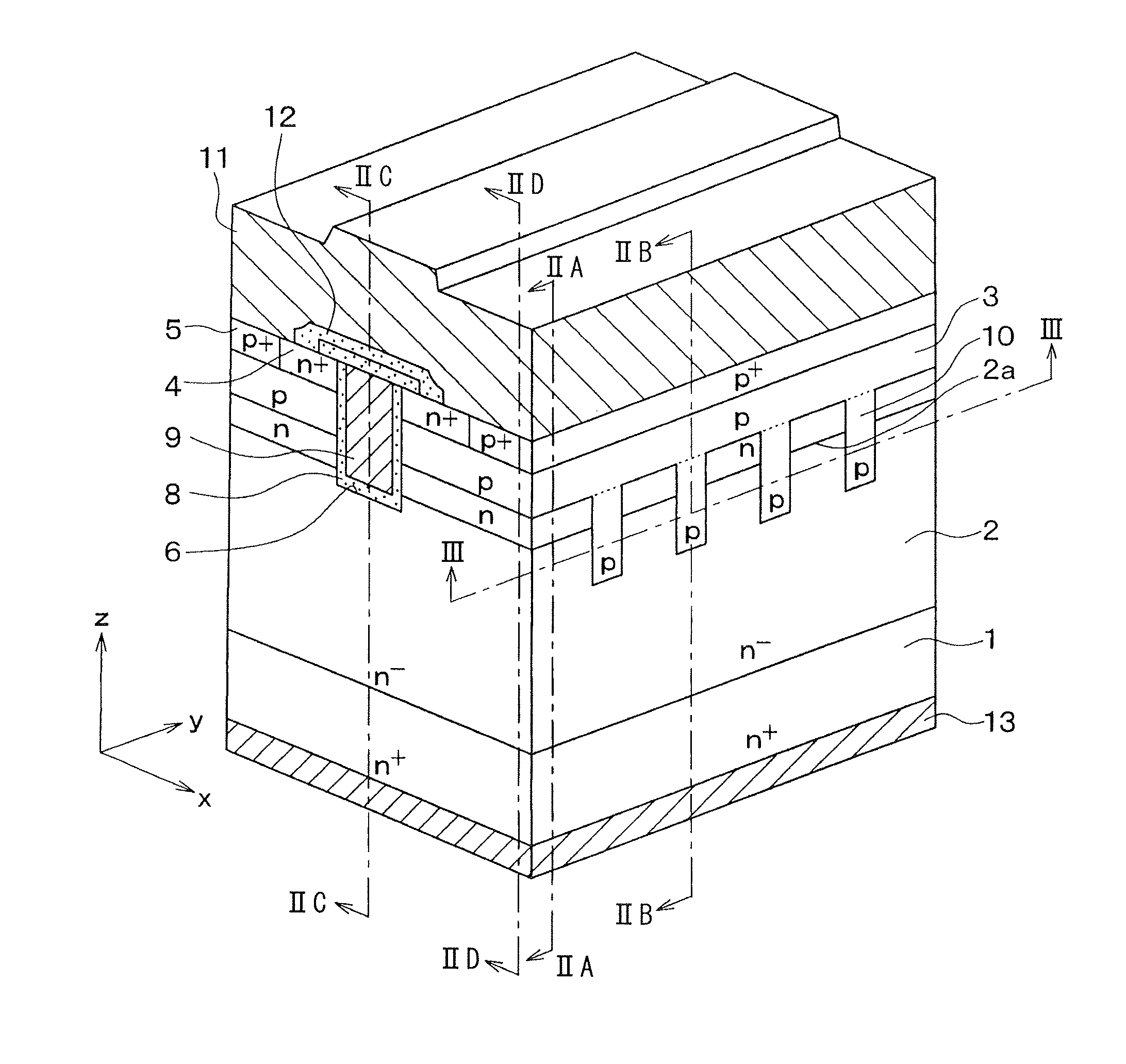
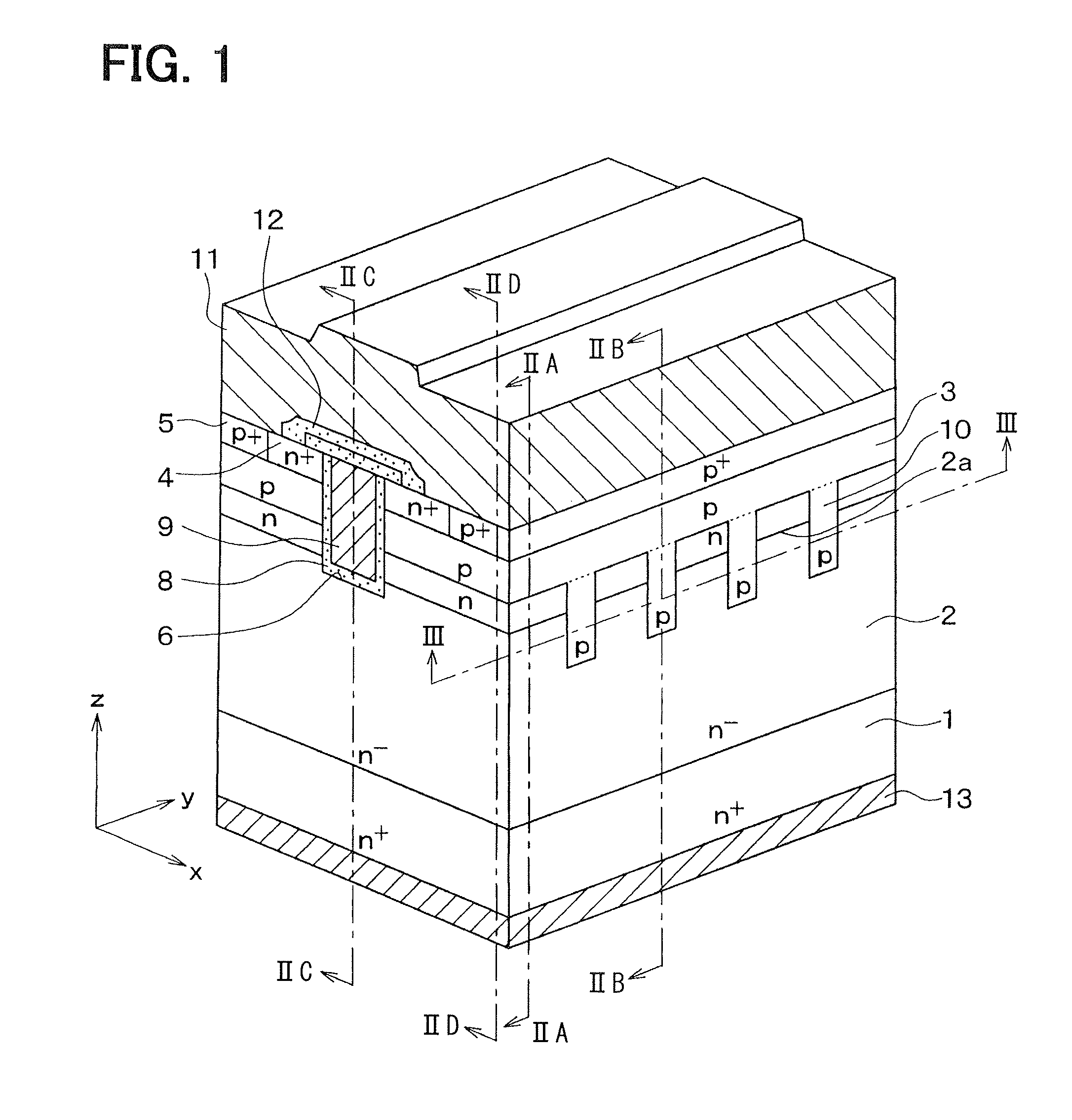
[0036]A SiC semiconductor device according to a first embodiment will be described with reference to FIG. 1 to FIG. 3. The SiC semiconductor device according to the present embodiment includes a MOSFET having an inversion trench gate structure.
[0037]Although only one cell of the MOSFET is shown in FIG. 1, MOSFETs having similar structures are arranged next to each other. FIG. 3 shows a cross section of three cells of MOSFET.
[0038]The MOSFET includes an n+ type substrate 1 made of SiC. The n+ type substrate 1 includes n type impurities such as phosphorus and has an n type impurity concentration of, for example, 1.0×1019 cm−3. The n type impurity includes, for example, phosphorus. The n+ type substrate 1 has a thickness of, for example, 300 μm. On a surface of the n+ type substrate 1, an n− type drift layer 2 made of SIC is disposed. The n− type drift layer 2 includes n type impurities such as phosphorus and has an n type impurity concentration of, for example, from 3.0×1015 cm−3 to 7...
second embodiment
[0070]A SiC semiconductor device according to a second embodiment will be described below.
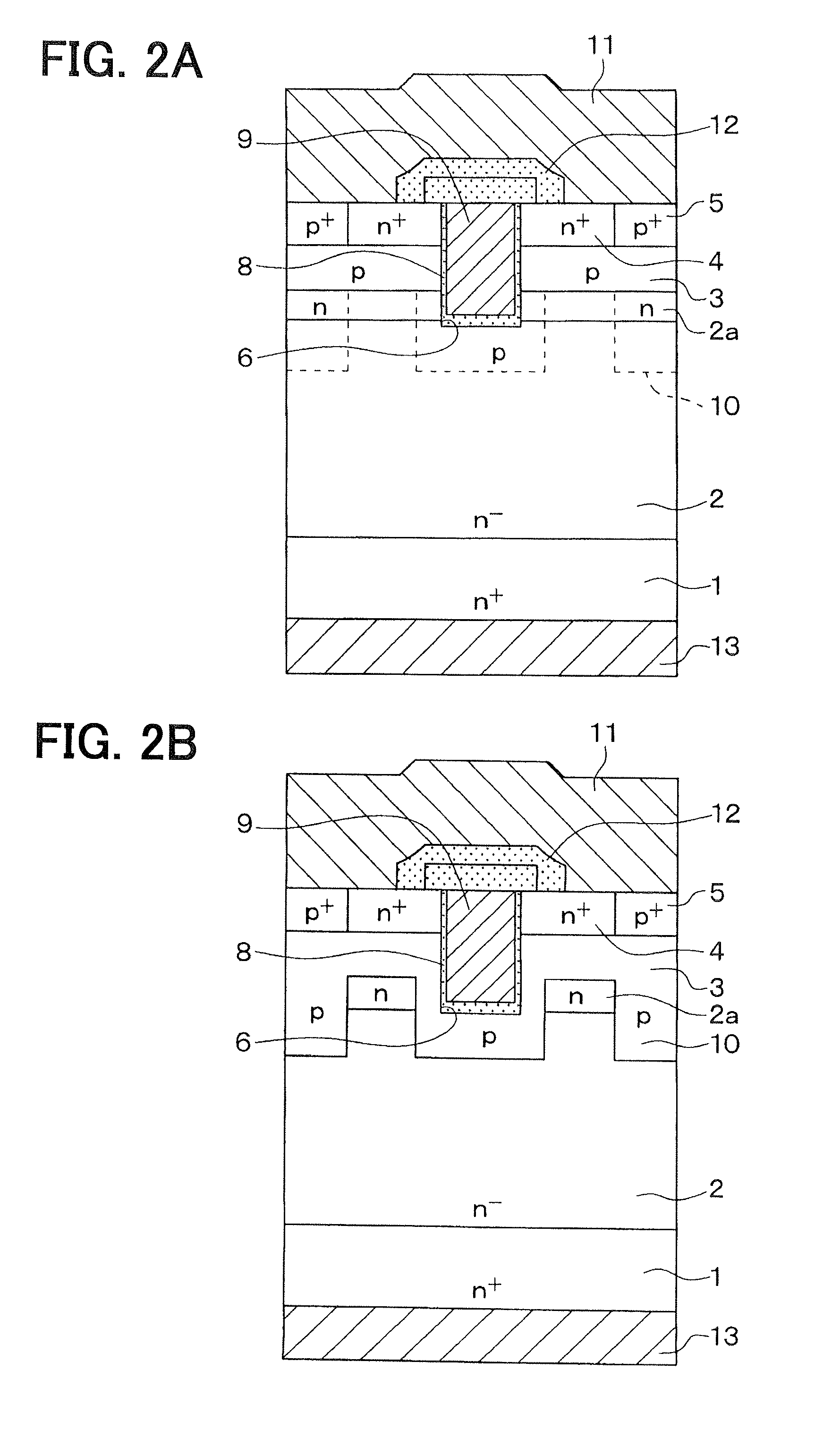
[0071]As shown in FIG. 7, FIG. 8A and FIG. 8B, in the SiC semiconductor device according to the present embodiment, the depth, the impurity concentration, and the layout of the p type deep layer 10 are similar to those of the first embodiment. The current diffusion layer 2a is partially disposed above the p type deep layer 10. The current diffusion layer 2a extends to a position at about 1 μm from the sidewall of the trench 6. Thus, each portion of the p type deep layer 10 being in contact with the trench 6 is in contact with the p type base region 3, and each portion of the p type deep layer 10 not being in contact with the trench 6 is in contact with the current diffusion layer 2a and is separated from the p type base region 3.
[0072]In the present configuration, compared with the first embodiment, the area of the current diffusion layer 2a can be increased. Thus, electric current can flow bet...
third embodiment
[0078]A SiC semiconductor device according to a third embodiment will be described with reference to FIG. 10.
[0079]FIG. 10 is a cross-sectional view showing a layout of a p type deep layer 10 in a trench gate MOSFET included in the SiC semiconductor device according to the present embodiment. The cross-section shown in FIG. 10 is taken along a line corresponding to the line III-III in FIG. 1.
[0080]In the present embodiment, the p type deep layer 10 includes a group of portions being in contact with the trench 6 and does not include a group of portions disposed between adjacent two lines of the trench 6.
[0081]The intervals of the portions of the p type deep layer 10 are increased in a direction perpendicular to the longitudinal direction of the trench 6. Thus, compared with the first embodiment and the second embodiment, the equipotential lines may enter upper positions between the portions of the p type deep layer 10, and electric field may concentrate at corners of a bottom of each...
PUM
 Abstract
Description
Claims
Application Information