Planarizing etch hardmask to increase pattern density and aspect ratio

a technology of planarizing etch and hardmask, which is applied in the field of integrated circuit fabrication, can solve the problems of complex integrated circuits, semiconductor industry facing the limitation of patterning sub-32 nm, etc., and achieve the effect of convenient removal

Inactive Publication Date: 2011-12-01
APPLIED MATERIALS INC
View PDF1 Cites 311 Cited by
  • Summary
  • Abstract
  • Description
  • Claims
  • Application Information

AI Technical Summary

Benefits of technology

[0008]Embodiments of the present invention provide a semiconductor device and a method for manufacturing a semiconductor device in a processing chamber. In one embodiment the method includes depositing over a substrate a first base material having a first set of interconnect features, filling an upper portion of the first set of interconnect features with an ashable material to an extent capable of protecting the first set of interconnect features from subsequent processes while being easily removable when desired, planarizing an upper surface of the first base material such that an upper surface of the ashable material filled in the first set of interconnect feature...

Problems solved by technology

Integrated circuits have evolved into complex devices that can include millions of transistors, capacitors and resistors on a single chip.
As device sizes shrink and pattern structure becomes more complex and difficult to manufacture, an etch hardmask is becoming more important as photoresists currently available are failing to meet the etching resi...

Method used


Image

  • Planarizing etch hardmask to increase pattern density and aspect ratio
  • Planarizing etch hardmask to increase pattern density and aspect ratio
  • Planarizing etch hardmask to increase pattern density and aspect ratio

Examples


Embodiment Construction

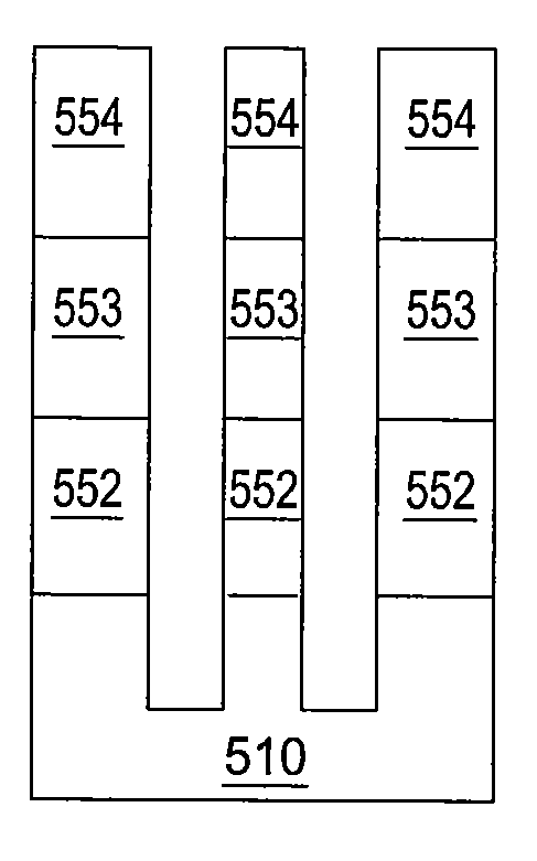
[0019]Embodiments of the present invention generally provide an improved patterning process for pattern density doubling in a desired film stacks for various applications such as metal contacts, source / drain contacts, capacitor, or shallow trench isolations. Embodiments described below also provide a planarizing etch hardmask process for improving integrated circuit device performance by nearly doubling aspect ratio of interconnect features in a desired height of film stacks.

Exemplary Hardware

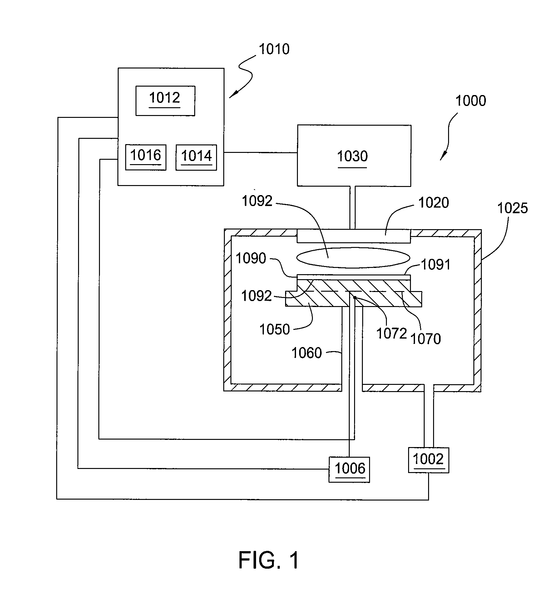
[0020]FIG. 1 is a schematic representation of a substrate processing system, system 1000, which can be used for features and / or amorphous carbon layer deposition according to embodiments of the present invention. Examples of suitable systems include the CENTURA® systems which may use a DxZ™ processing chamber, PRECISION 5000® systems, PRODUCER™ systems, such as the PRODUCER SE™ processing chamber and the PRODUCER GT™ processing chamber, all of which are commercially available from Applied Mater...


PUM


Abstract

Methods for manufacturing a semiconductor device in a processing chamber are provided. In one embodiment, a method includes depositing over a substrate a first base material having a first set of interconnect features, filling an upper portion of the first set of interconnect features with an ashable material to an extent capable of protecting the first set of interconnect features from subsequent processes while being easily removable when desired, planarizing an upper surface of the first base material such that an upper surface of the ashable material filled in the first set of interconnect features is at the same level with the upper surface of the first base material, providing a substantial planar outer surface of the first base material, depositing a first film stack comprising a second base material on the substantial planar outer surface of the first base material, forming a second set of interconnect features in the second base material, wherein the second set of interconnect features are aligned with the first set of interconnect features, and removing the ashable material from the first base material, thereby extending a feature depth of the semiconductor device by connecting the second set of interconnect features to the first set of interconnect features. In another embodiment, a method includes providing a base material having a first film stack deposited thereon, wherein the base material is formed over the substrate and having a first set of interconnect features filled with an amorphous carbon material, the first film stack comprising a first amorphous carbon layer deposited on a surface of the base material, a first anti-reflective coating layer deposited on the first amorphous carbon layer, and a first photoresist layer deposited on the first anti-reflective coating layer, and patterning a portion of the first photoresist layer by shifting laterally a projection of a mask on the first photoresist layer relative to the substrate a desired distance, thereby introducing into the first photoresist layer a first feature pattern to be transferred to the underlying base material, wherein the first feature pattern is not aligned with the first set of interconnect features.

Description

BACKGROUND OF THE INVENTION[0001]1. Field of the Invention[0002]Embodiments of the present invention generally relate to the fabrication of integrated circuits and particularly to planarizing etch hardmask processes for obtaining an increased aspect ratio feature in a desired film stacks or increasing the pattern density for a given region.[0003]2. Description of the Related Art[0004]Integrated circuits have evolved into complex devices that can include millions of transistors, capacitors and resistors on a single chip. The evolution of chip design continually requires faster circuitry and greater circuit density. The demand for faster circuits with greater circuit densities imposes corresponding demands on the materials used to fabricate such integrated circuits.[0005]Hardmasks are being used for almost every step in integrated circuit manufacturing processes for both front-end and back-end processes. As device sizes shrink and pattern structure becomes more complex and difficult t...

Claims


Application Information

Patent Timeline
IPC IPC(8): H01L21/302H01L23/52G03F7/20H01L21/30
CPCH01L21/02115H01L21/0337H01L21/0332H01L21/02274H01L21/0273H01L21/0274H01L21/31
Inventor SEAMONS, MARTIN JAYLEE, KWANGDUK DOUGLASCHAN, CHIUREILLY, PATRICKRATHI, SUDHA
Owner APPLIED MATERIALS INC
Why Eureka
Try Eureka