
Relaxation and transfer of strained material layers

a strained, layer technology, applied in the direction of polycrystalline material growth, crystal growth process, after-treatment details, etc., can solve the problems of strained heteroepitaxial films, buckling suppression does not show satisfying results, and the material quality of layers grown thereon is affected

Active Publication Date: 2011-12-01
SOITEC SA
View PDF3 Cites 10 Cited by
  • Summary
  • Abstract
  • Description
  • Claims
  • Application Information

AI Technical Summary

Benefits of technology

The patent describes a method for creating strained material layers on a patterned seed substrate. The method involves patterning the seed substrate, growing a strained material layer on the patterned seed substrate, transferring the strained material layer to an intermediate substrate, and relaxing the strained material layer by a heat treatment. The resulting strained material layer has higher crystalline quality and lower strain levels compared to conventional methods. The method also allows for the use of low-cost substrates and the formation of strained material islands with greater thickness.

Problems solved by technology

However, when films are formed by heteroepitaxy on substrates with different lattice constants and different coefficients of thermal expansion as compared to the ones of the films, detrimental effects on material quality of layers grown on the films are caused by compressive / tensile strain and the corresponding generation of defects like dislocations, cracks, plastic relaxation, etc., that result in detrimental effects on the material quality of layers grown thereon.
Presently used methods for the relaxation of strained heteroepitaxial films, however, often do not show satisfying results with respect to the suppression of buckling, etc.
Moreover, the transfer of heteroepitaxial films grown on a seed (growth) substrate, including some seed layer to another substrate that is to be used for the further manufacture of a particular semiconductor, raises the problem of maintaining the heteroepitaxial films intact, in general, and, in particular, removing the seed substrate without damaging the heteroepitaxial films.

Method used


Image

  • Relaxation and transfer of strained material layers
  • Relaxation and transfer of strained material layers
  • Relaxation and transfer of strained material layers

Examples


Embodiment Construction

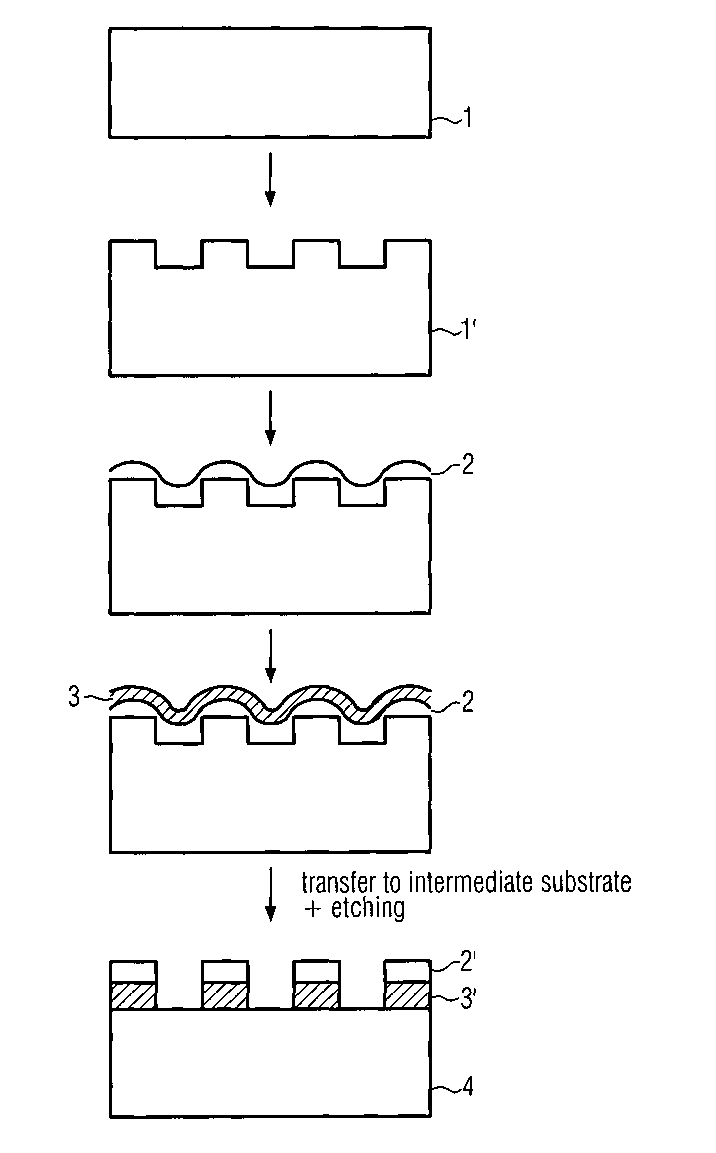
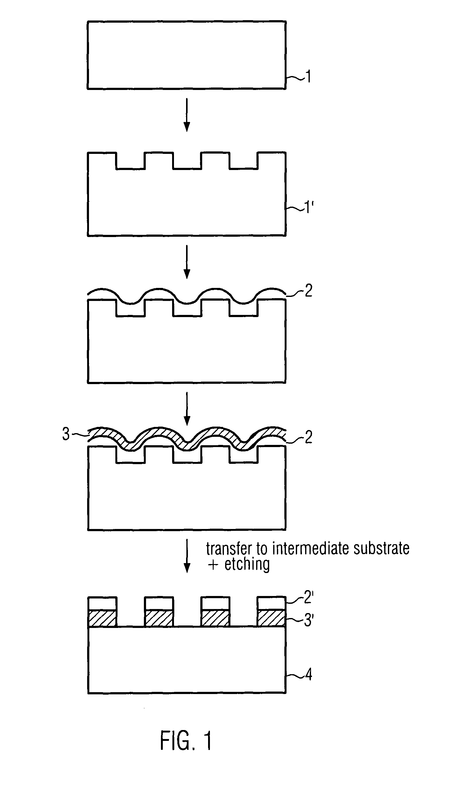
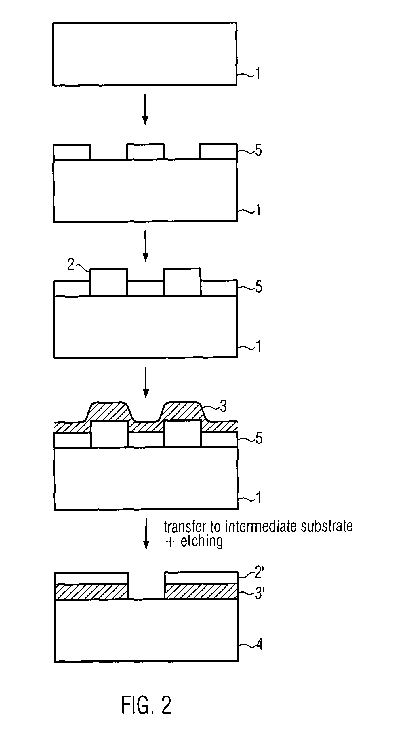
[0053]In the following, two alternative embodiments of the herein disclosed method for the formation of at least partially relaxed strained material layers are described with reference to FIGS. 1 and 2. As shown in FIG. 1, a seed substrate 1 is provided for the growth of a strained material layer. The seed substrate 1 may, e.g., be a sapphire substrate or a silicon substrate. The seed substrate 1 is patterned by etching to obtain seed substrate islands 1′ separated by recesses. The seed substrate islands may, e.g., be sized to 1×1 millimeters and spaced apart at about 10 to 1000 micrometers. The recesses may have a depth of about 1 micrometer.

[0054]After patterning of the seed substrate 1, epitaxy of a strained material, e.g., InGaN with 10% Indium, is performed up to a thickness of the strained material layer 2 of about 250 nanometers. In order to improve the crystalline quality of the strained material layer 2, a buffer layer (not shown) may be deposited on the patterned seed subs...


PUM

PropertyMeasurementUnit
thicknessaaaaaaaaaa
area sizeaaaaaaaaaa
temperaturesaaaaaaaaaa

Abstract

The present invention relates to a method for the formation of an at least partially relaxed strained material layer, the method comprising the steps of providing a seed substrate; patterning the seed substrate; growing a strained material layer on the patterned seed substrate; transferring the strained material layer from the patterned seed substrate to an intermediate substrate; and at least partially relaxing the strained material layer by a heat treatment.

Description

CROSS-REFERENCE TO RELATED APPLICATIONS[0001]This is a national phase entry under 35 U.S.C. § 371 of International Patent Application PCT / EP2010 / 000090, filed Jan. 11, 2010, published in English as International Patent Publication WO 2010 / 094371 A2 on Aug. 26, 2010, which claims the benefit under Article 8 of the Patent Cooperation Treaty to European Patent Application Serial No. 09290100.8, filed Feb. 19, 2009, the entire disclosure of each of which is hereby incorporated herein by this reference.TECHNICAL FIELD[0002]The present invention relates to the field of compliant substrates employed in the manufacture of semiconductor devices and, in particular, to the relaxation of strained material islands and the transfer of the at least partially relaxed strained material islands to some support substrate that can suitably be used for further semiconductor manufacture processes.BACKGROUND[0003]The growth of thin films on substrates by heteroepitaxy is an important manufacturing step in...

Claims


Application Information

Patent Timeline
Patent Type & Authority Applications(United States)
IPC IPC(8): H01L21/762H01L29/02
CPCC30B29/403C30B33/02C30B33/06H01L21/02381H01L21/76254H01L21/0243H01L21/02458H01L21/0254H01L21/02664H01L21/0242H01L21/20H01L21/762
Inventor LETERTRE, FABRICEFAURE, BRUCEGUENARD, PASCAL
Owner SOITEC SA
Learn More