
Relaxation and transfer of strained material layers
a strained, layer technology, applied in the direction of polycrystalline material growth, crystal growth process, after-treatment details, etc., can solve the problems of strained heteroepitaxial films, buckling suppression does not show satisfying results, and the material quality of layers grown thereon is affected
Patent Information
- Authority / Receiving Office
- US · United States
- Patent Type
- Patents(United States)
- Current Assignee / Owner
- Publication Date
- 2015-05-26
Smart Images
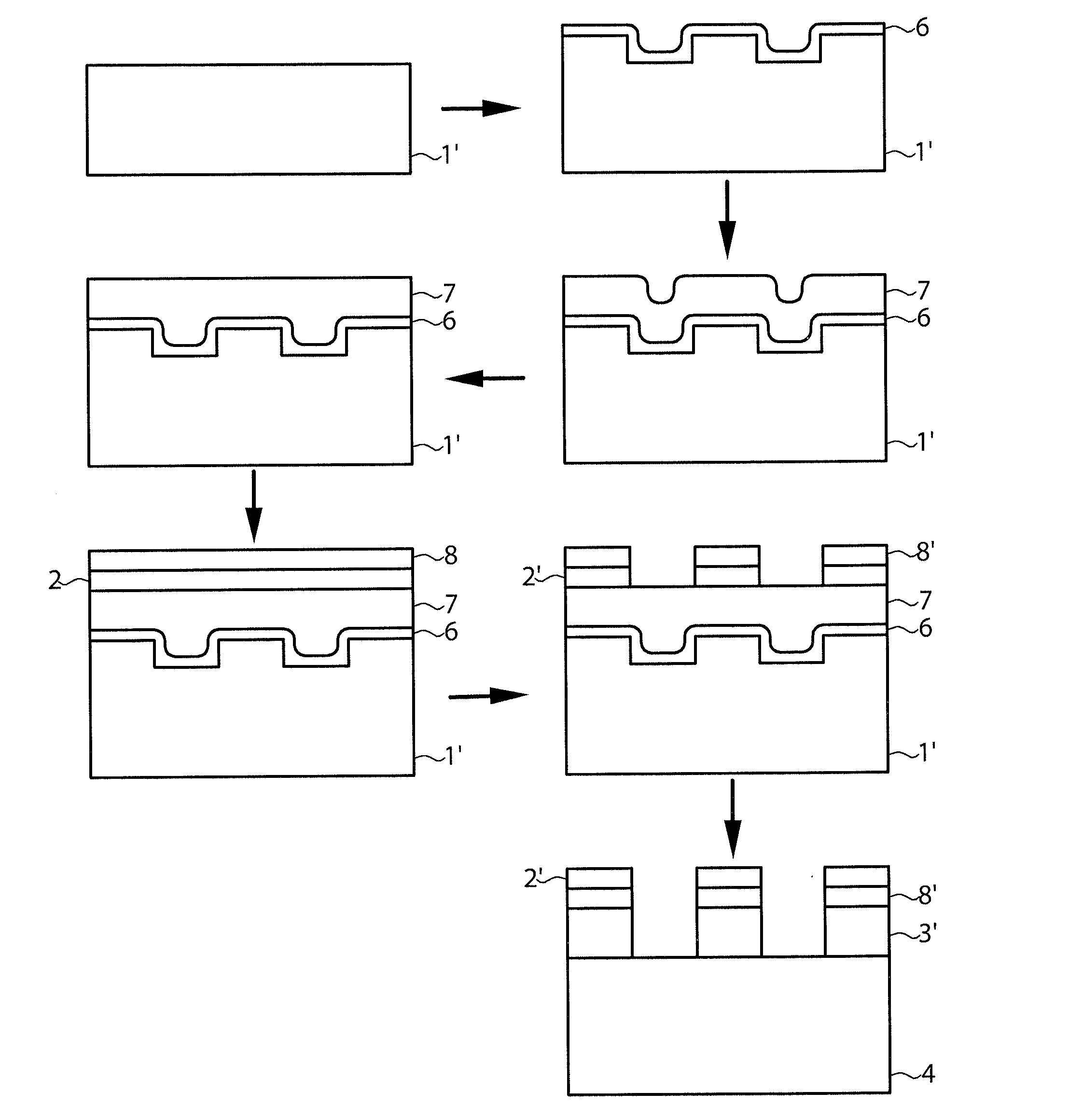
Figure 1 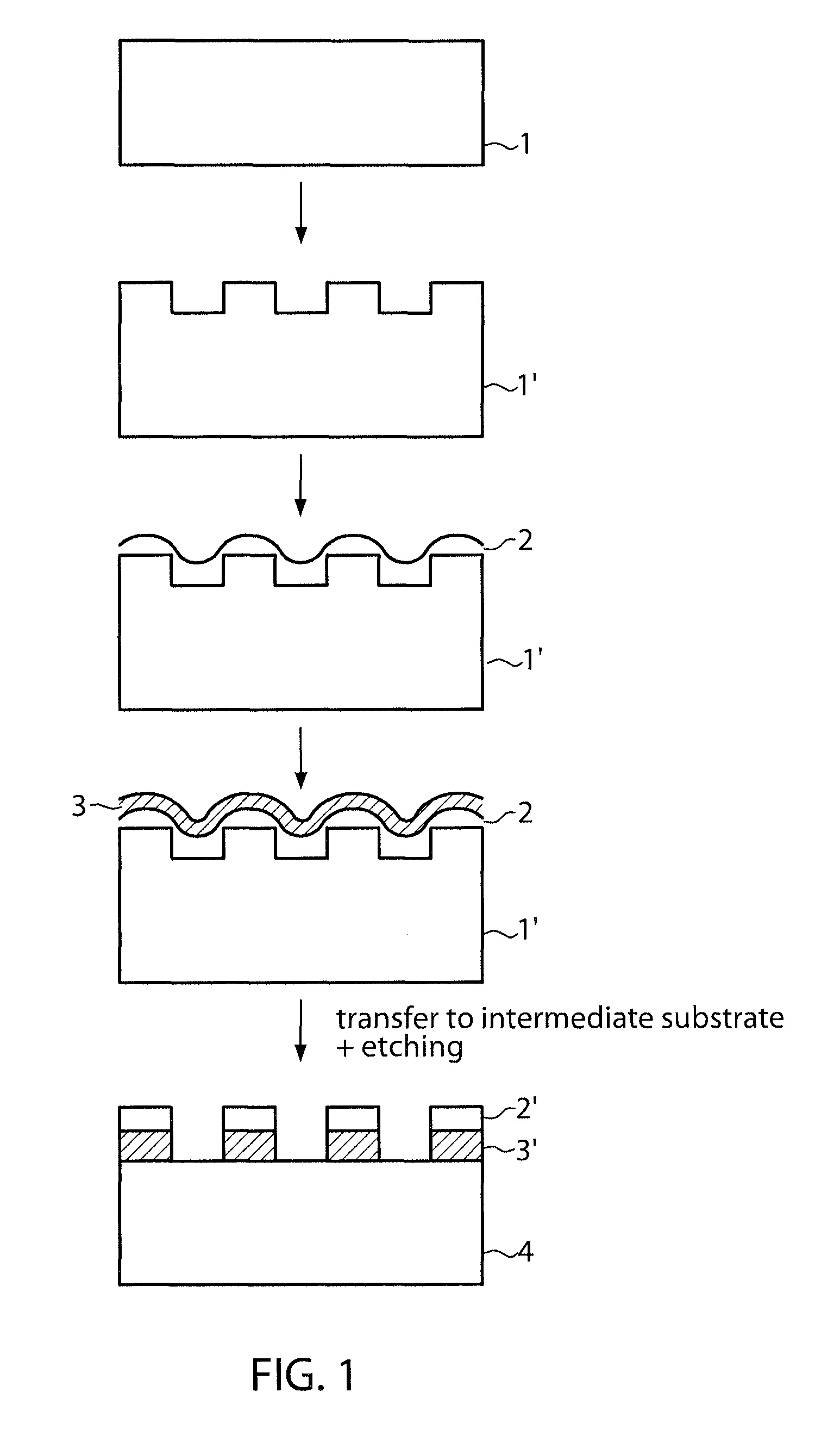
Figure 2 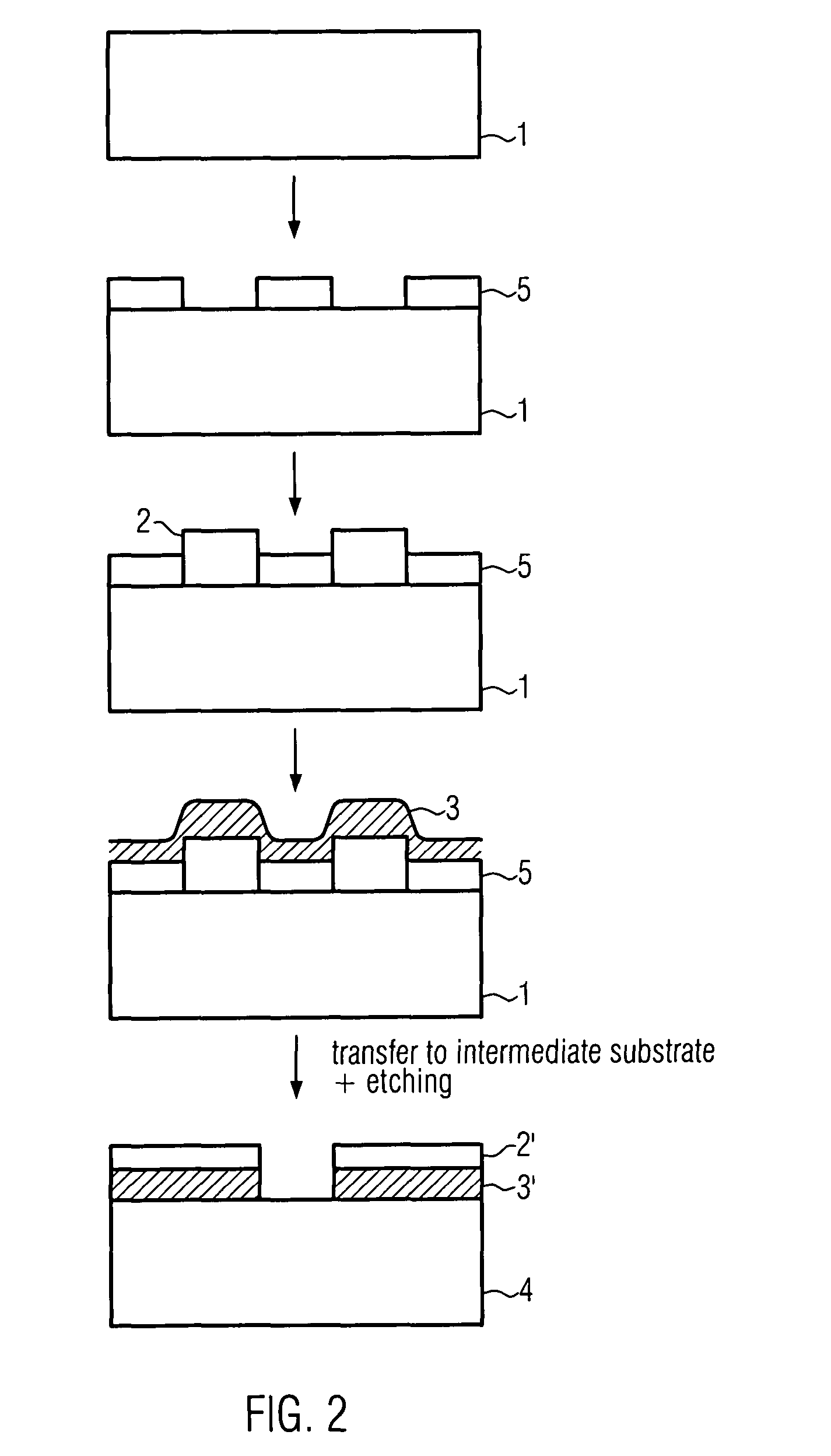
Figure 3
Abstract
Description
CROSS-REFERENCE TO RELATED APPLICATIONS
[0001] This is a national phase entry under 35 U.S.C. §371 of International Patent Application PCT / EP2010 / 000090, filed Jan. 11, 2010, published in English as International Patent Publication WO 2010 / 094371 A2 on Aug. 26, 2010, which claims the benefit under Article 8 of the Patent Cooperation Treaty to European Patent Application Serial No. 09290100.8, filed Feb. 19, 2009, the entire disclosure of each of which is hereby incorporated herein by this reference.TECHNICAL FIELD
[0002] The present invention relates to the field of compliant substrates employed in the manufacture of semiconductor devices and, in particular, to the relaxation of strained material islands and the transfer of the at least partially relaxed strained material islands to support substrates that can suitably be used for further semiconductor manufacture processes.BACKGROUND
[0003] The growth of thin films on substrates by heteroepitaxy is an important manufacturing step in the ...
Examples
Embodiment Construction
[0053]In the following, two alternative embodiments of the herein disclosed method for the formation of at least partially relaxed strained material layers are described with reference to FIGS. 1 and 2. As shown in FIG. 1, a seed substrate 1 is provided for the growth of a strained material layer 2. The seed substrate 1 may be, e.g., a sapphire substrate or a silicon substrate. The seed substrate 1 is patterned by etching to obtain seed substrate islands 1′ separated by recesses. The seed substrate islands 1′ may be, e.g., sized to 1 mm×1 mm and spaced apart at about 10 micrometers to 1000 micrometers. The recesses may have a depth of about 1 micrometer.
[0054]After patterning of the seed substrate 1, epitaxy of a strained material, e.g., InGaN with 10% indium, is performed up to a thickness of the strained material layer 2 of about 250 nanometers. In order to improve the crystalline quality of the strained material layer 2, a buffer layer (not shown) may be deposited on the patterne...