Finfet-compatible metal-insulator-metal capacitor

a metal-insulator and capacitor technology, applied in the direction of diodes, semiconductor devices, electrical apparatus, etc., can solve problems such as planar capacitors, and achieve the effect of increasing capacitan

Active Publication Date: 2011-12-08
GLOBALFOUNDRIES US INC
View PDF8 Cites 168 Cited by
  • Summary
  • Abstract
  • Description
  • Claims
  • Application Information

AI Technical Summary

Problems solved by technology

Thus, the conventional planar capacitor that employs an upper portion of a semiconductor substrate as a lower plate cannot be formed on a substrate including finFETs.

Method used


Image

  • Finfet-compatible metal-insulator-metal capacitor
  • Finfet-compatible metal-insulator-metal capacitor
  • Finfet-compatible metal-insulator-metal capacitor

Examples


first embodiment

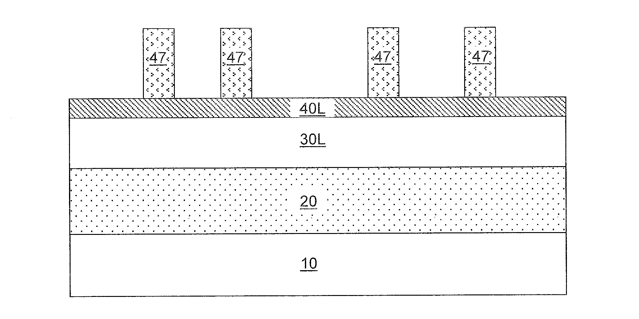
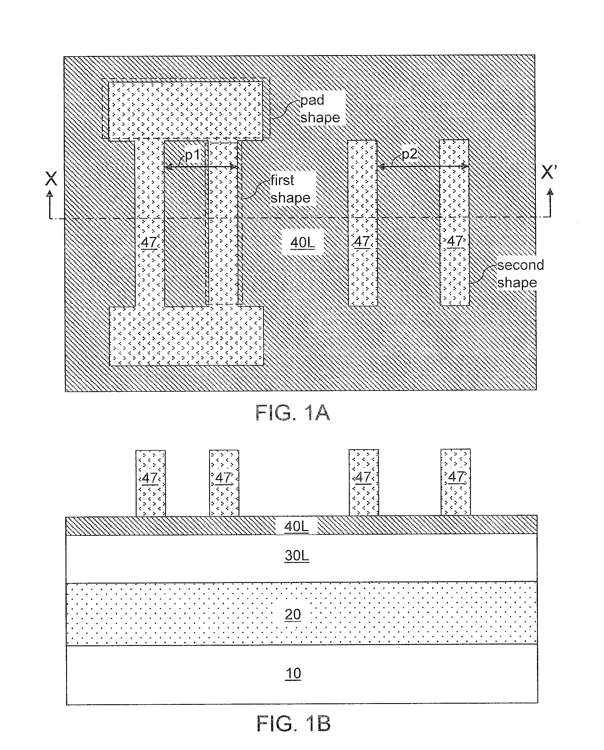
[0040]Referring to FIGS. 1A and 1B, a first exemplary semiconductor structure according to the present invention includes a substrate containing a vertical stack of a handle substrate 10, an insulator material layer 20, and a top semiconductor layer 30L. The handle substrate 10 may include a semiconductor material, an insulator material, a conductive material, or a combination thereof. The handle substrate 10 can provide mechanical support for the insulator material layer 20 and the top semiconductor layer 30L.

[0041]The insulator material layer 20 includes an insulator material such as silicon oxide, silicon nitride, silicon oxynitride, or a combination thereof. The insulator material layer 20 provides electrical isolation between the top semiconductor layer 30L and the handle substrate 10. The thickness of the insulator material layer 20 can be from 30 nm to 2 microns, and typically from 50 nm to 500 nm, although lesser and greater thicknesses can also be employed.

[0042]The top sem...

second embodiment

[0065]Referring to FIGS. 8A and 8B, a second exemplary semiconductor structure according to the present invention is shown after deposition of the MOL dielectric layer 90 and formation of various contact via structures (92, 94, 96, 98). The MOL dielectric layer 90 is omitted from the top-down view of FIG. 8A for clarity. The second exemplary semiconductor structure can be derived from the first exemplary semiconductor structure by omitting the formation of the fin cap dielectric layer 40L. Correspondingly, the at least one first dielectric fin cap portion 40A and the at least one second dielectric fin cap portion 40B are not formed. Each first fin structure 33A includes a sub-portion of a first semiconductor material portion 30A, and each second fin structure 3313 includes a second semiconductor material portion 30B. The top surfaces of the at least one first semiconductor material portion 30A contacts a bottom surface of the lower conductive plate 50. The top surfaces of the at lea...

third embodiment

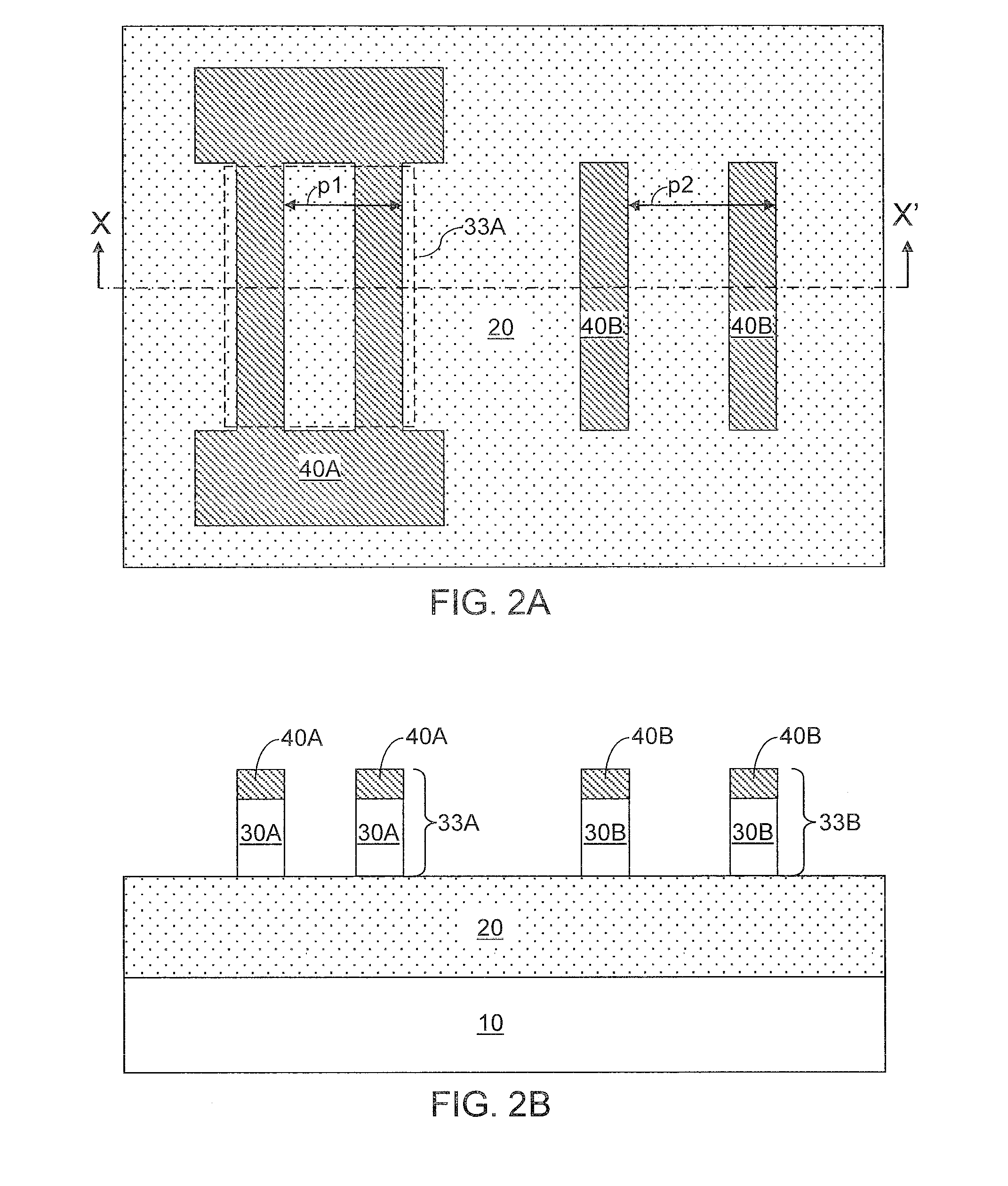
[0066]Referring to FIGS. 9A and 9B, a third exemplary semiconductor structure according to the present invention is derived from the first exemplary semiconductor structure of FIGS. 1A and 1B by etching through unmasked portions of the fin cap dielectric layer 40L and the top semiconductor layer 30L and subsequently etching into upper portions of the insulator material layer 20. The insulating material layer 20 including patterned recessed areas is herein referred to as a patterned insulating material layer 20′. The first masking layer 47 is subsequently removed. The recess depth rd, which is the vertical distance between the topmost surfaces of the patterned insulating material layer 20′ and the recessed surfaces of the patterned insulating material layer 20′ can be from 1% to 99%, and typically from 10% to 90% of the thickness of the insulating material layer 20 prior to patterning.

[0067]The patterned insulating material layer 20′ includes a planar portion, which is herein referre...


PUM


Abstract

At least one semiconductor fin for a capacitor is formed concurrently with other semiconductor fins for field effect transistors. A lower conductive layer is deposited and lithographically patterned to form a lower conductive plate located on the at least one semiconductor fin. A dielectric layer and at least one upper conductive layer are formed and lithographically patterned to form a node dielectric and an upper conductive plate over the lower conductive plate as well as a gate dielectric and a gate conductor over the other semiconductor fins. The lower conductive plate, the node dielectric, and the upper conductive plate collectively form a capacitor. The finFETs may be dual gate finFETs or trigate finFETs. A buried insulator layer may be optionally recessed to increase the capacitance. Alternately, the lower conductive plate may be formed on a planar surface of the buried insulator layer.

Description

BACKGROUND[0001]The present invention relates to a semiconductor structure including a metal-insulator-metal capacitor (MIMCAP) compatible with finFET structures, and methods of manufacturing the same.[0002]Capacitors are employed as passive components in a semiconductor chip. Capacitors are employed to decouple power supplies, to form a memory element, to form an RC delay circuit, and / or to provide various other circuit functions. Because capacitors tend to take up a significant circuit area, compact high capacitance capacitors are desirable for highly-integrated advanced semiconductor chips. At the same time, the number and complexity of additional processing steps for adding capacitors should be minimized in order to contain the total processing cost and to minimize the total processing time for semiconductor chips.[0003]The advent of finFETs, i.e., field effect transistors formed on semiconductor fins having a height greater than the width, alters the processing steps of convent...

Claims


Application Information

Patent Timeline
Patent Type & Authority Applications(United States)
IPC IPC(8): H01L27/108H01L21/8234
CPCH01L21/823431H01L27/0805H01L27/0629
Inventor HAENSCH, WILIFRIED E.KULKARNI, PRANITAYAMASHITA, TENKO
Owner GLOBALFOUNDRIES US INC
Why Eureka
Try Eureka