Optical Waveguide and Optical Waveguide Module

a technology of optical waveguides and modules, applied in the field of optical waveguides and optical waveguide modules, can solve the problems of crosstalk countermeasures, increasing the number of lines, and other problems in conventional electric wiring, and achieve the effects of low loss, high accuracy of mounting, and easy realization of highly accurate elements

Inactive Publication Date: 2011-12-08
HITACHI CHEM CO LTD
View PDF3 Cites 30 Cited by
  • Summary
  • Abstract
  • Description
  • Claims
  • Application Information

AI Technical Summary

Benefits of technology

[0027]The effects obtained by typical embodiments of the invention disclosed in the present application will be briefly described below.
[0028]According to the present invention, the convex member having the convex step is provided so as to be planarly overlapped with the mirror part of the waveguide, the optical element is provided with the concave part, and the convex member and the concave part are mated with each other, thereby easily realizing highly-accurate mounting of elements. Since highly accurate mounting can be achieved, the element and the waveguide can be coupled to each other with low loss. Therefore, the optical waveguide module capable of realizing efficient high-quality optical transmission with small power consumption can be provided.
[0029]Furthermore, when the convex step is formed from a material similar to that of the core layer of the optical waveguide, the convex step can be formed by photolithography patterning in the manufacturing process of the optical waveguide. Since this can be formed by a continuous process, in addition to achieving the short-time manufacturing, the positional misalignment with respect to the core layer of the optical waveguide can be reduced compared with the positional misalignment of the case in which a separate member is mounted. Accordingly, the optical waveguide having high coupling efficiency with respect to the optical element can be formed.
[0030]FIG. 1A is a perspective view showing a schematic configuration of the optical waveguide module according to the first embodiment of the present invention;
[0031]FIG. 1B is a plan view showing the schematic configuration of the optical waveguide module according to the first embodiment of the present invention;
[0032]FIG. 1C is a cross-sectional view showing the cross-sectional structure taken along the A-A line of FIG. 1B;

Problems solved by technology

When increase in the capacity of systems is further advanced in the future, in the case of a device which processes information of Tbit / s or more, the problems of the number of lines, crosstalk countermeasures, and others will become more and more serious in conventional electric wiring.
Moreover, it is effective to change signal transmission lines to optical lines also in video equipment such as video cameras and commercial equipment such as PCs and mobile phones other than the above-described router / switch since increase in the speed / capacity of video signal transmission between monitors and terminals is required in the implementation of high-definition images in the future, and the problems such as countermeasures against signal delay and noise become notable in conventional electric wiring.

Method used


Image

  • Optical Waveguide and Optical Waveguide Module
  • Optical Waveguide and Optical Waveguide Module
  • Optical Waveguide and Optical Waveguide Module

Examples


first embodiment

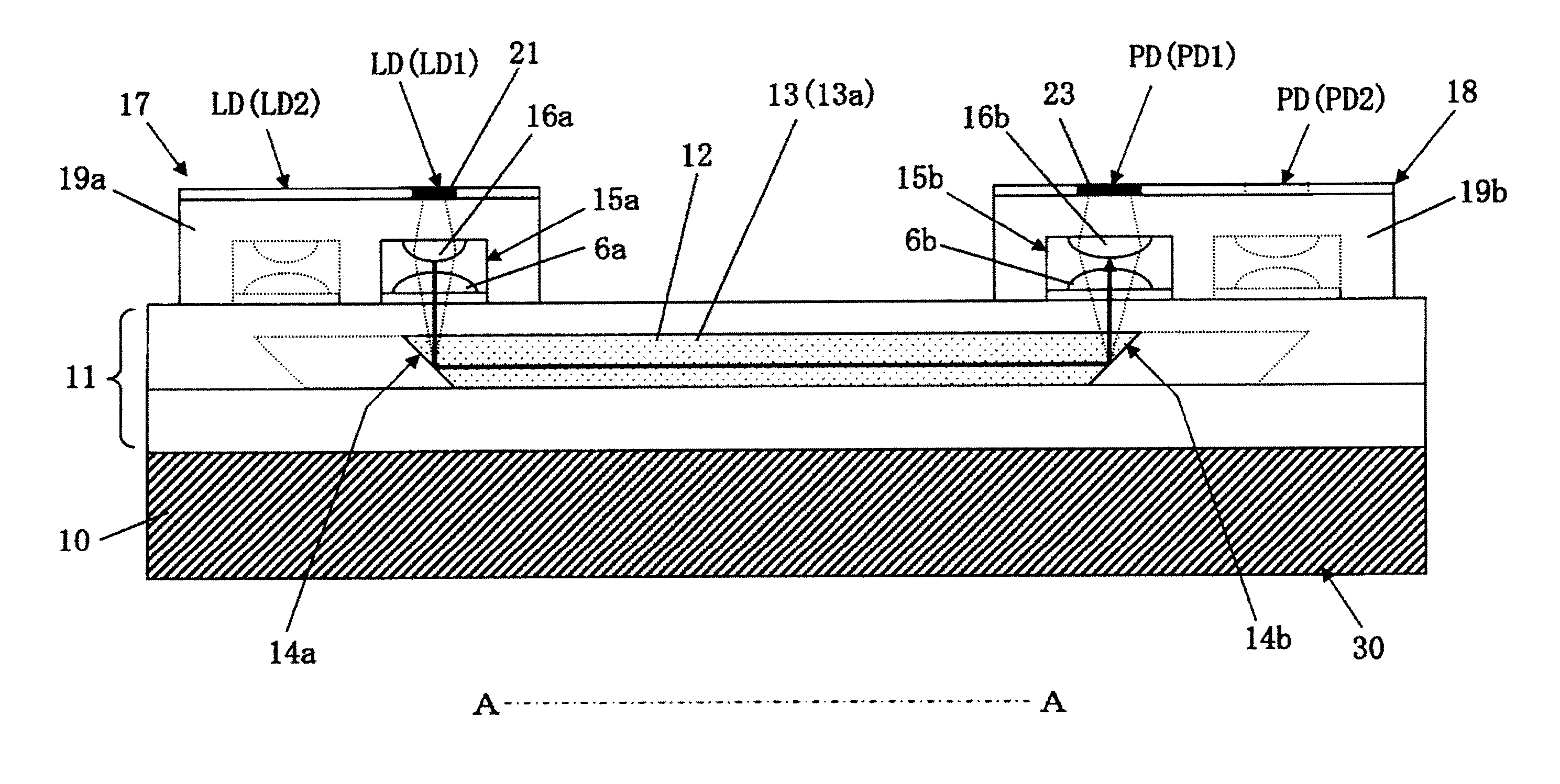
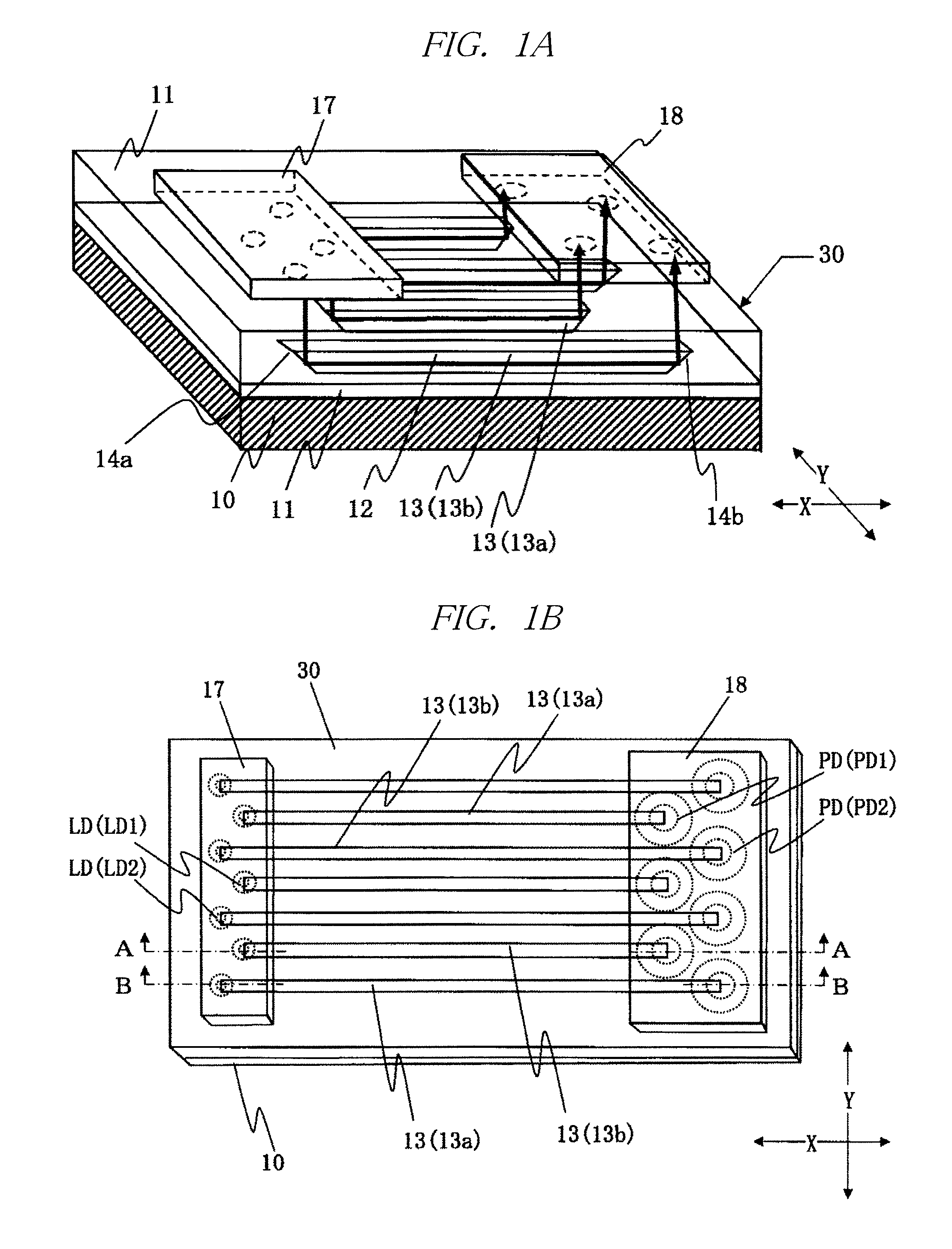
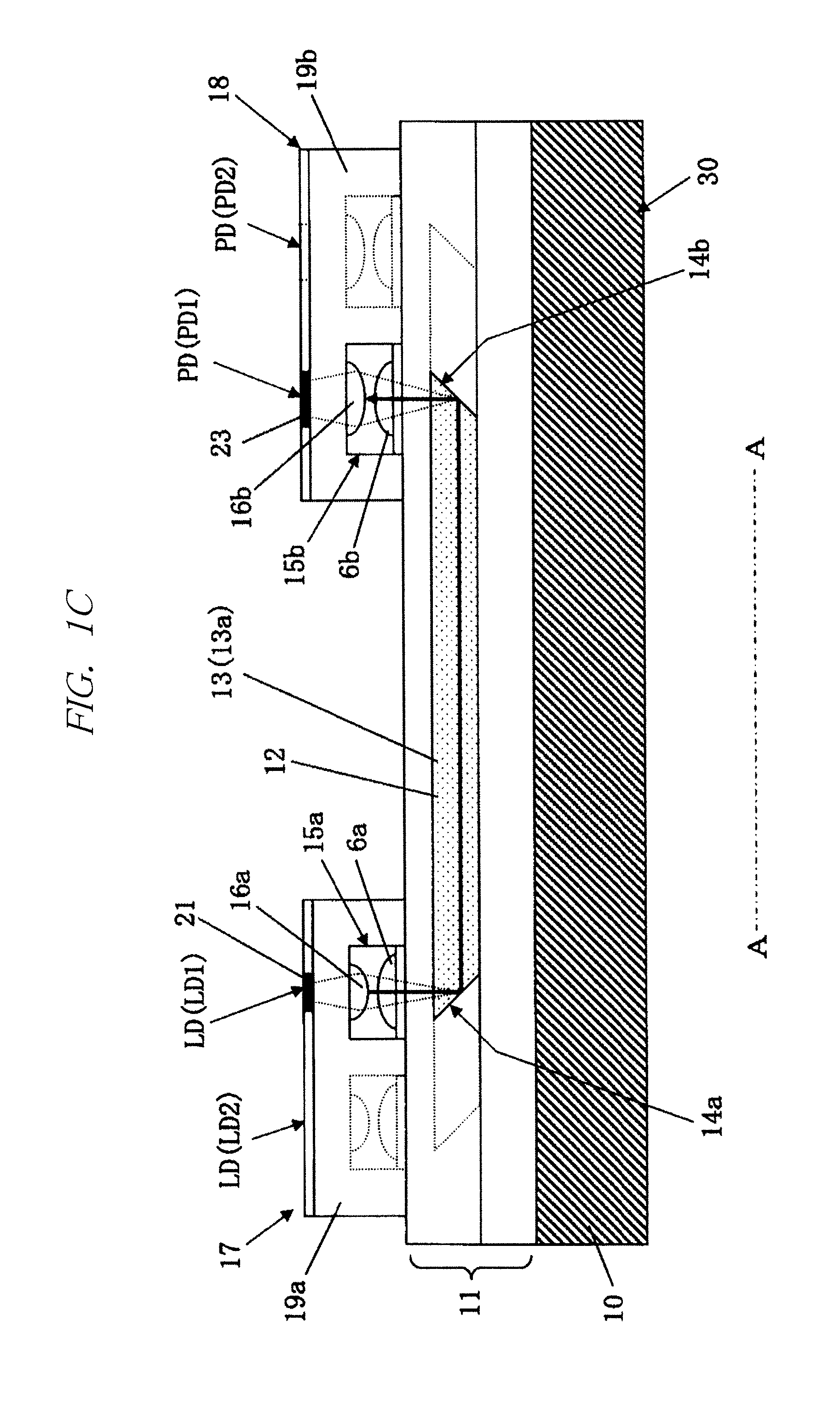
[0052]In the present first embodiment, an example in which the present invention is applied to an optical waveguide module having: a laser diode array in which a plurality of laser diodes are disposed; a photo diode array in which a plurality of photo diodes are disposed; and an optical waveguide substrate on which a plurality of optical waveguides optically connecting them are disposed will be described.

[0053]FIG. 1A to FIG. 1E are drawings relating to the optical waveguide module according to the first embodiment of the present invention, in which

[0054]FIG. 1A is a perspective view showing a schematic configuration of the optical waveguide module,

[0055]FIG. 1B is a plan view showing the schematic configuration of the optical waveguide module,

[0056]FIG. 1C is a cross-sectional view showing the cross-sectional structure taken along the A-A line of FIG. 1B,

[0057]FIG. 1D is a cross-sectional view showing the cross-sectional structure taken along the B-B line of FIG. 1B, and

[0058]FIG. ...

second embodiment

[0111]FIG. 5A to FIG. 5C are drawings relating to an optical waveguide module according to the second embodiment of the present invention, in which

[0112]FIG. 5A is a plan view (top view) showing a schematic configuration of the optical waveguide module,

[0113]FIG. 5B is a cross-sectional view showing the cross-sectional structure taken along the C-C line of FIG. 5A, and

[0114]FIG. 5C is a cross-sectional view showing the cross-sectional structure taken along the D-D line of FIG. 5A.

[0115]The optical waveguide module of the present second embodiment basically has a configuration similar to that of the above-described first embodiment and has a difference in configuration described below.

[0116]In the above-described first embodiment, the optical waveguide substrate 30 having the single-layer optical waveguide array has been described.

[0117]On the other hand, as shown in FIG. 5A to FIG. 5C, the optical waveguide substrate 30 of the present second embodiment has a multilayer structure in ...

third embodiment

[0125]FIG. 6A and FIG. 6B are drawings relating to an optical waveguide module according to the third embodiment of the present invention, in which

[0126]FIG. 6A is a cross-sectional view showing a schematic configuration of the optical waveguide module, and

[0127]FIG. 6B is a cross-sectional view showing the state in which illustration of optical element arrays (laser diode array and photo diode array) in FIG. 6A is omitted.

[0128]Herein, an optical waveguide made of a material which can be bent at an arbitrary curvature and having flexibility is used for the part of the waveguide.


PUM


Abstract

An optical waveguide module which satisfies highly-accurate and stable optical connection between optical elements and optical waveguides and can be easily fabricated is provided. As means for it, in an optical waveguide module having: an optical waveguide surrounded by a cladding layer and provided with a mirror part formed of a tapered surface on a first end side; an optical element having a concave part in a first surface of a semiconductor substrate; and a convex member provided on the cladding layer so as to be planarly overlapped with the mirror part, the convex member is mated with the concave part of the optical element.

Description

TECHNICAL FIELD[0001]The present invention relates to an optical waveguide and an optical waveguide module and more particularly relates to the techniques effectively applied to an optical waveguide module serving as a terminal in the transmission of high-speed optical signals which are transmitted / received between chips or boards with using optical waveguides as wiring media between devices or in a device such as a data processing device.BACKGROUND ART[0002]Recently, in the field of information and telecommunications, the communication traffic for transmitting / receiving large-volume data at high speed by using light has been rapidly developing, and fiber-optic networks have been expanded for comparatively long distances of several km or more such as a backbone network, metro network and access network. In the future, further changing of signal wiring to optical wiring is effective also for the extremely short distances such as a rack-to-rack distance (several cm to several hundreds...

Claims


Application Information

Patent Timeline
Patent Type & Authority Applications(United States)
IPC IPC(8): G02B6/32G02B6/26
CPCG02B6/4214G02B6/43G02B6/4249G02B6/122G02B6/42
Inventor MATSUOKA, YASUNOBUSUGAWARA, TOSHIKI
Owner HITACHI CHEM CO LTD
Why Eureka
Try Eureka